Growth & Synthesis
Chemical depositions of thin films View all
GBM Graphene-based materials
Synthesis of graphene layers and other 2D materials. Especially using Chemical Vapor Deposition techniques on catalytic metal substrates to obtain large area uniform films. Some techniques are also available for the transfer and functionalization of those graphene based or 2D materials to tune their chemico-physical surface properties.
ALD Atomic Layer Deposition

ALD is an advanced thin film manufacturing process for mainstream applications expanding beyond semiconductor processing. It achieves new levels of performance in Li-ion batteries, fuel cells, logic and memory devices, light-harvesting energy (i.e. surface passivation layers, buffer layers in solar cells) but also encapsulation of polymers.
CSD Chemical solution deposition

CSD is a growth technique of thin films, self-assembled nanomaterials or nanocomposite thin films where chemical solution is first deposited on substrates and then chemical precursors are transformed into solid compounds. A wide range of functional oxides and inorganic compounds are grown by CSD leading to epitaxial or polycrystalline structures.
CVD Chemical Vapour Deposition

It is a chemical process used to produce high quality, high-performance, solid materials. The process is often used in the semiconductor industry to produce thin films. In typical CVD, the wafer (substrate) is exposed to one or more volatile precursors, which react and/or decompose on the substrate surface to produce the desired deposit.
Thermal treatments View all
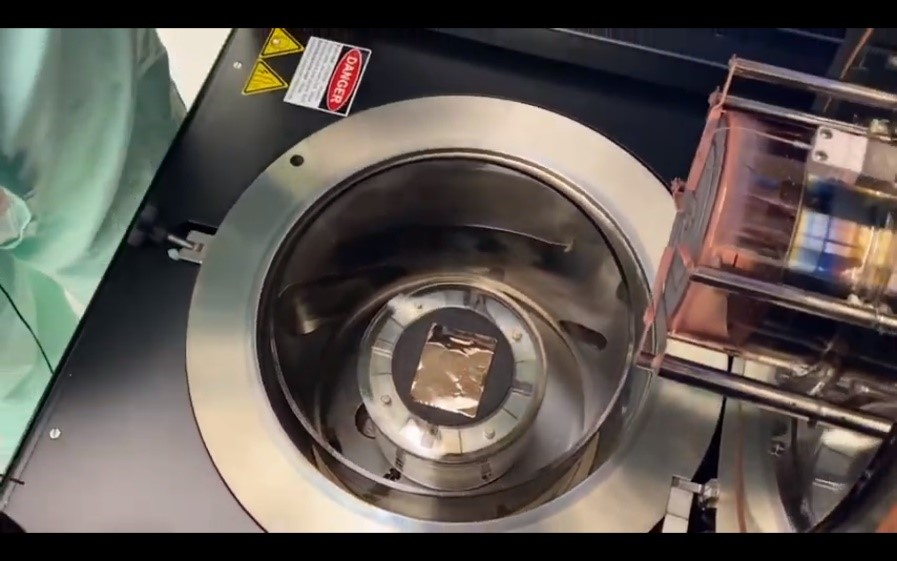
FLA Flash lamp annealing
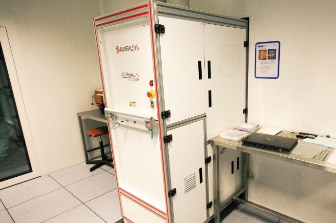
The furnace uses flash lamps for rapid processing of materials at high temperature (implant annealing, oxidation , nitridation, ohmic contact…), particularly for semiconductor wafers.
SSR Solid State Reaction
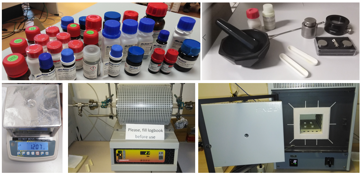
The solid-state reaction route is the most widely used method for the preparation of polycrystalline solids from a mixture of solid starting materials.
TP Thermal processes

Processes involving exposure of (usually) semiconductors samples to oxidizing or inert ambient at high temperature (300- 1150C). For example, O2 or H2O ambient are used to grow silicon dioxide on Si. Inert ambient (N2, Ar) are used to densify layers or to activate and redistribute dopant impurities. N2/H2 is used for aluminum sintering.
Synthesis of nanoparticles View all
AD Aerosol deposition

The aerosol deposition process allows controllable size generation and deposition of aerosol particles of metals, e.g. Au, Ag, In, Pb, Pd, Cu. The size range of the aerosol particles is 8 - 100 nm with a narrow distribution. Aerosols can be randomly deposited on any substrate with densities up to 50 µm-2.
GIN Growth of inorganic nanocrystals
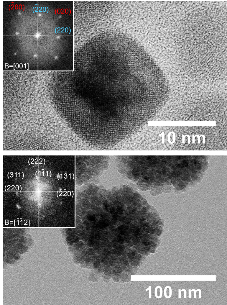
The nanochemistry facility exploits elaborate bottom-up colloidal chemistry approaches that harness nanoscale size and shape-guiding mechanisms to afford various kinds of inorganic nanocrystals with tunable response (cf. semiconducting, plasmonic, magnetic).
MICS Multiple Ion Cluster Source
We offer a multiple ion-cluster source operating in ultra-high vacuum devoted to the fabrication and characterization of highly controlled nanoparticles. They are produced in gas phase with high purity and controlled size, structure and stoichiometry and they can be collected in the desired coverage on arbitrary surfaces for different uses.
FSP Flame Spray Pyrolysis

FSP allows the production of a broad range of nanostructured materials in the form of nanocrystalline powders with particle sizes ranging from few nanometers up to 10 nm. These materials include metal oxides (e.g. SiO2, TiO2 and Al2O3), complex oxides (e.g. YSZ and ITO), noble metals and nanocomposites (e.g. alumina or titania supported Pt).
CBD Cluster Beam Deposition

In CBD, aggregates formed in the gas-phase are processed in a molecular beam source so to form a collimated beam of particles that once intercepted by a substrate can be used to grow thin films of nanostructured materials. Nanocomposites are produced by co-deposition from multiple sources. Accessible materials are metals, carbon, metal-oxides.
Physical depositions of thin films View all
PVDS PVD sputtering
Physical vapor deposition (PVD) by sputtering is a process whereby a material is sputtered from a solid target and deposited on a substrate as a film or coating, with thicknesses from sub-nm to several microns, in mono-layered, multi-layered, or multi-graduated structures and well-controlled morphology.
PLD Pulsed Laser Deposition

PLD is widely used to grow thin films of complex oxides and other inorganic and organic materials. It is a simple and versatile technique based in the congruent ablation of a solid material irradiated by an ultraviolet laser.
EBE e-beam evaporation
E-Beam evaporation is a physical vapor deposition (PVD) technique whereby an intense electron beam is generated from a filament and steered via electric and magnetic fields to strike the source material (e.g. pellets of Au) and vaporize it within a vacuum environment.
TE Thermal evaporation
Thermal evaporation is a simple high-vacuum physical vapor deposition method for depositing thin films of materials (few Å to few hundred nm). The technique involves the joule-heating of a solid source material that evaporates and deposits on the substrate. Common deposited materials are Al, Ag, Ni, Cr, Au, In, among many others.
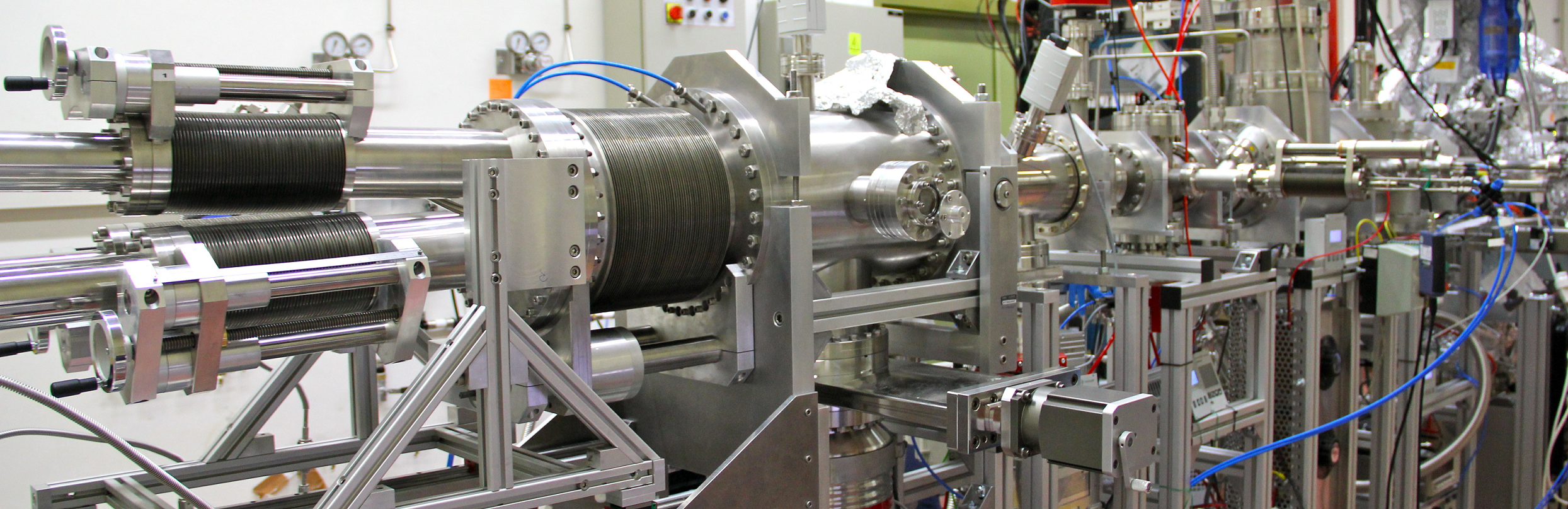
MBE Molecular Beam Epitaxy

MBE allows growth of high quality semiconductors, oxides and organic epitaxial layers, with crystal structure commensurate with the substrate. It is used to build nanostructures (quantum dots, nanowires), layered heterostructures for lasers, photodetectors, LED and optoelectronic devices.
MS Magnetron sputtering

This is a simple physical method to deposit, in form of thin film or multilayers, a wide variety of materials from simple metals to complex inorganic structures, between few Angstroms and hundreds of nanometers. The technique is based on the evaporation of solid surface by field-accelerated ions of a heavy gas that are focused by a magnetic field.
Soft matter synthesis View all
SMP Soft matter preparation

Different nanochemical methodologies are offered to prepare nanomaterials (nanoparticles, nanowires, nanodots, self-assembled monolayers, films, nanoparticles, liposomes, emulsions, vesicles, etc). Among the systems that can be prepared are organic, hybrid organic-organic organic-inorganic, polymeric and biomaterial systems.

