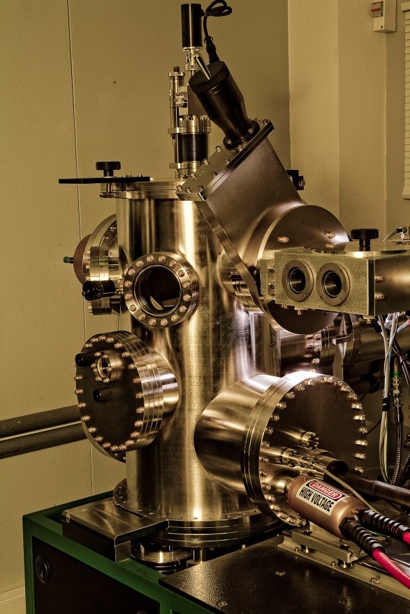
E-Beam evaporation is a physical vapor deposition (PVD) technique whereby an intense electron beam is generated from a filament and steered via electric and magnetic fields to strike the source material (e.g. pellets of Au) and vaporize it within a vacuum environment. At some point as the source material is heated via this energy transfer its surface atoms will have sufficient energy to leave the surface, traverse the vacuum chamber and coat a substrate positioned above the evaporating material.
The advantage of this method over thermal evaporation is the possibility to use higher energies into the material to be evaporated, which leads to the formation of thin films with a higher density and consequently with an increased adhesion to the substrate. This method is also good for posterior lift-off processes, and is the way to obtain thin films with the highest purity. By using a multiple crucible E-beam gun, several different materials can be deposited without breaking the vacuum and thus avoiding interlayer contamination.
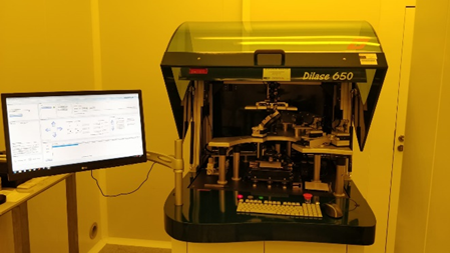
Direct Writing lithography (DWL) is a Maskless lithography technique in which the pattern is transferred directly onto the surface of the wafer without the need of a photomask. A direct laser writer, guided by a control computer, “writes” the patterns that conform one layout level directly onto the resist-covered substrates.
RIE is used to etch various materials under vacuum in the presence of reactive ions. The sample to be etched is placed in a vacuum chamber and gas is injected into the process chamber via a gas inlet in the top electrode. The lower electrode is negatively biased and a single RF plasma source determines both the ion density and their energy.
Displacement Talbot Lithography is a contactless method to produce regular features over large areas. A 3D diffraction pattern is formed below a mask with a periodic pattern. A photoresist-coated substrate is moved vertically through this pattern so the effective dose is integrated in space and time forming a collapsed version of the pattern.
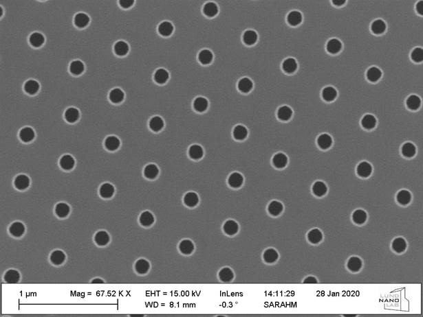
In SEM a beam is scanned over a sample surface while a signal from secondary or back-scattered electrons is recorded. SEM is used to image an area of the sample with nanometric resolution, and also to measure its composition, crystallographic phase distribution and local texture.
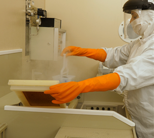
A set of classical microelectronic processes for pattern transfer through etching of thin films than are co-adjuvant to the functional materials of a given sytem under study in the micro or nano domain. It includes wet and dry etching of all those ancillary dielecric or conducting materials.