Growth of inorganic nanocrystals
Growth & Synthesis (Synthesis of nanoparticles)
The nanochemistry facility will offer cost-efficient, easily scaled-up and accessible nanocrystals fabrication for the ever demanding field of nanosciences.
The user-oriented approach entails exploitation of new solution-based “bottom-up”, assembly mechanisms that can accomplish structural control at the nanoscale, either by free-energy changes or kinetics. The facility aims to lead to paradigms for assembling functional systems that accomplish desirable properties, either unavailable or prohibitively expensive by using “top-down” approaches (e.g. state-of-the-art lithography techniques applied to semiconductor nanostructures).
Wet-chemistry techniques for the preparation and characterization of colloidal nanocrystals, with controlled size, shape and composition will be ready available for users in need of nanomaterials with semiconducting, plasmonic, and magnetic natures. However, any material request outside the palette of these systems will be also considered for further development.
The users will be either delivered with the requested nanomaterial or be trained by the laboratory scientists and technicians to undertake synthesis of nanosized colloidal crystals of desired chemical composition (e.g. chalcogenide, noble metal, oxide, halide) and adjustable geometrical characteristics (size and shape). For this, colloidal chemistry techniques will be made available, for nanocrystals’ synthesis and purification, including chemical hoods, equipped with vacuum-inert gas lines (Schlenk type), digital temperature control of the growth conditions, PID-controlled furnaces for post-synthesis treatment and anaerobic glove-boxes for handling and manipulating air-sensitive reagents in the course of each user-based project.
Also consider
SEM Scanning Electron Microscopy

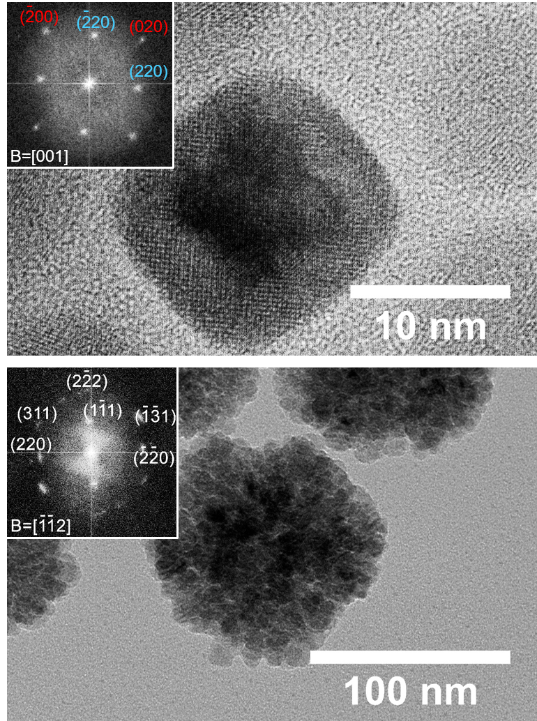
TEM Transmission Electron Microscopy

OS Optical spectroscopy

XRD X-Ray Diffraction

SGSEP Structural and ground-state electronic properties


