Thermal processes
Growth & Synthesis (Thermal treatments)
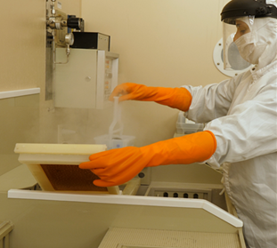
Silicon oxidation is the exposure of silicon (or polysilicon) to the action of gas oxidants (O2- termed dry oxidation, H2O – termed wet oxidation) at high temperatures (800-1150C). It is usually an atmospheric pressure process run on large tubular furnaces holding up to several tens of substrates. Part of the silicon of the surface (layer) is consumed and transformed in SiO2 so the starting thickness of the silicon layer is reduced (roughly 50% of the thickness of the obtained silicon dioxide); it can be used for thinning silicon micro-nanostructures. Oxide thicknesses of a few nanometers to two micron can be obtained depending on the temperature, time and ambient of the oxidation process. Dry oxidation is best suited for thin oxides and wet oxidation is best suited for thicker ones.
Diffusion is the process by which a species moves in a given environment due to a spatial gradient in concentration. Diffusion processes in the field of microelectronics are those that allow the spatial and in-depth definition of the substrate regions with different dopant species (mainly, boron and phosphorus) that are in the base the semiconductor industry. Depending on the depth pursued high temperatures and long times may be needed.
An annealing is a thermal process in which the substrates are exposed to different temperatures, times and environments depending on the pursued objective such as the predeposition of doping species (as an alternative to ion implantation), the post-implant annealing for impurities activation, the fluidization of interlevel dielectric layers, annealing of aluminum layers for contacts formation and the densification of different deposited layers.

Instruments datasheets
Also consider
RIE Reactive Ion Etching

UVL Ultra Violet Lithography

Standard depos. Standard chemical and physical deposition cleanroom/lab processes
XPS X-ray Photoelectron Spectroscopy

Standard etching Standard dry/wet patterning cleanroom/lab processes