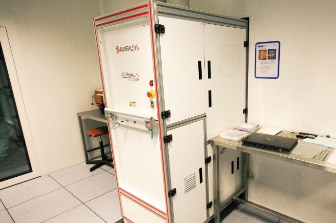
Flash lamp annealing
Growth & Synthesis (Thermal treatments)
The flash lamp furnace allows processing materials without submitting them to long temperature ramping time, shortening dramatically thermal processes. The infrared lamp furnaces can reach temperature up to 1450°C and for duration up to 1 hour at 1200°C. Some high temperature systems can run process at 2000°C for 1 hour. The temperature ramp rate may reach up to 100°C/s, with faster system allowing to heat the sample from both side.
The process may be performed in controlled gaseous atmosphere and with a pressure ranging between atmospheric pressure down to 10-6 Torr.
The main applications of the process are for:
- Rapid Thermal Annealing (RTA)
- Implant annealing
- Contact annealing (III-V and SiC)
- Rapid Thermal Oxidation (RTO)
- Rapid Thermal Nitridation (RTN)
- Annealing of piezoelectric and pyroelectric materials
- Getter activation
- Rapid Thermal Evaporation (RTE)
- Selenization (CIGS solar cells)
- Sol-gel densification and crystallization
- Etc.
@
provided at NFFA-Europe laboratories by:
@
provided by:
Instruments datasheets
LUND + MAX IV
Sweden
Rovak Flash lamp annealed (FLA)
EURONANOLAB
France
FLA at EURONANOLAB - IEMN
EURONANOLAB
France
FLA at EURONANOLAB - FEMTO-ST
EURONANOLAB
France
FLA at EURONANOLAB - IMM
@
provided at NFFA-Europe laboratories by:
@
provided by:
Also consider
Structural & Morphology Characterization
SEM Scanning Electron Microscopy

In SEM a beam is scanned over a sample surface while a signal from secondary or back-scattered electrons is recorded. SEM is used to image an area of the sample with nanometric resolution, and also to measure its composition, crystallographic phase distribution and local texture.
Nano to Micro/Macro
UVL Ultra Violet Lithography

Ultraviolet lithography also known as optical or photolithography is the most commonly used patterning technique in microfabrication. A photosensitive material (photoresist) is spin-coated onto the substrate to be patterned. The photoresist is illuminated with UV light through a photomask which contains the relevant geometric patterns.
Growth & Synthesis
CBD Cluster Beam Deposition

In CBD, aggregates formed in the gas-phase are processed in a molecular beam source so to form a collimated beam of particles that once intercepted by a substrate can be used to grow thin films of nanostructured materials. Nanocomposites are produced by co-deposition from multiple sources. Accessible materials are metals, carbon, metal-oxides.
Nano to Micro/Macro
Thixotropy Thixotropy
This technology allows to investigate the thixotropic behavior of complex fluids, i.e., the dependence of viscosity on time after changes in the flow conditions.

