Cluster Beam Deposition
Growth & Synthesis (Synthesis of nanoparticles)
CBD is a special kind of Physical Vapor Deposition method, where aggregates formed in the gas-phase are processed in a molecular beam source so to form a collimated beam of particles. This can be finally used to grow thin films of nanostructured materials once it is intercepted by a substrate.
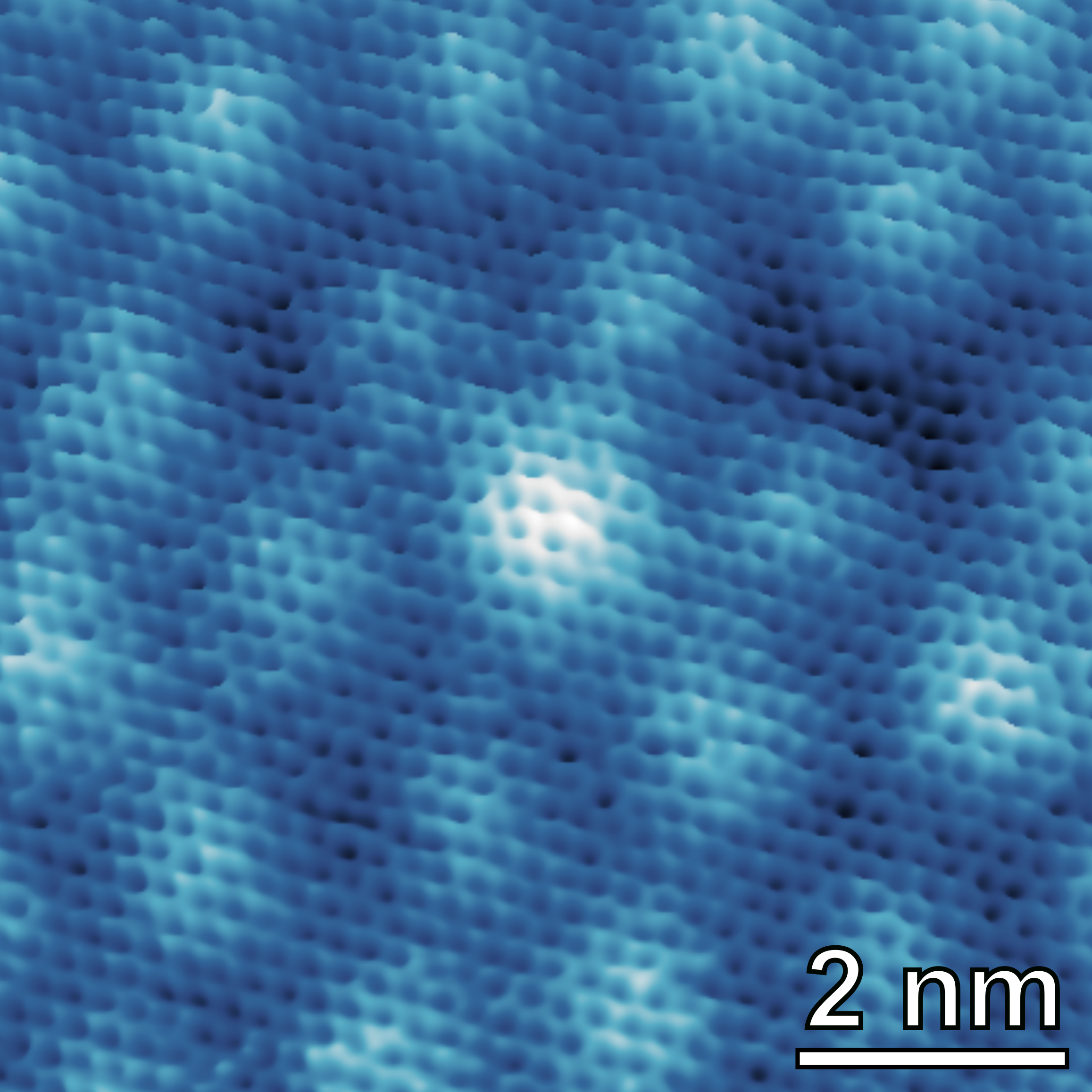
In the supersonic-source implementation of the technique (SCBD), the film is formed by random stacking of the nanoparticles that owing to their relatively low kinetic-energy (i.e. the energy per atom is small compared to cohesive energy) are soft-landing on the substrate and thus retain much of their gas-phase structure. The material can thus inherit structural properties from the deposited clusters which act as building blocks for the nanostructured film.
Aerodynamic separation and focusing effects allow the preparation of intense beams with controlled particle size distribution. Owing to the high-collimation and well-defined directionality of the beam, SCBD can be used to produce micro-structures and high-resolution patterns with nanostructured material by simple interposition of a non-contact stencil mask between the source and the substrate.
The technique is UHV compatible and easily integrated with different deposition methods or multiple sources. When the PMCS (Pulsed Micro-plasma Cluster Source) is applied as a particle beam source, high deposition rates are achieved and deposition of nanostructured films of several microns thickness is obtained within minutes. Large areas can be covered by rastering the substrate in front of the particle beam. The source can produce metal, carbon, oxide clusters and arbitrary mixtures of these ultrafine particles (typically below 5nm in diameter) can be deposited to produce nano-composite films by simultaneously operating multiple CBD sources. Among metals, Mg, Al, Ti, Ni, Ag, Au, Zr, W are the most commonly used; Zn0, TiO2 have been demonstrated for gas-phase oxide particles, but post-deposition oxidation is generally adopted.

Instruments datasheets
Also consider
SEM Scanning Electron Microscopy

XPS X-ray Photoelectron Spectroscopy

TEM Transmission Electron Microscopy

RS Raman spectroscopy

STM Scanning Tunneling Microscopy