Optical lithography is a fast patterning technique as all patterns are transferred to the photoresist through the mask in parallel. This requires that the relevant photomasks are already available or that they also need to be fabricated usually by electron beam lithography (in the case of non-standard patterns). Standard photomasks are made of fused quartz coated with a layer of chromium. During mask fabrication Cr is etched away where the geometric patterns need to be. This way UV light has a clear path through the mask, so as to expose the photosensitive resist and transfer the patterns, while Cr acts as a light-stop layer to prevent the illumination of the rest of the photoresist. The most common UV light wavelengths used in standard photolithography are the 436 nm ("g-line"), the 405 nm ("h-line") and the 365 nm ("i-line"), all being spectral lines of an Hg lamp. The achievable resolutions at these wavelengths go down to below 1 μm. There are different modes one can perform standard photolithography either with the mask being in contact with the resist-coated sample (contact lithography) or leaving a small gap (proximity lithography) each one having its own advantages and disadvantages.
Achievable resolutions: 2.0 µm in soft contact mode, 1.0 µm in hard contact mode
MJB3: high-precision alignment stage accurate to 0.5 µm and a brightfield microscope equipped with 5X, 10X and 25X objectives
MA25: simultaneous double side exposure and manual operation of wafers and small samples, alignment accuracy between upper and lower side of the wafer of <2 microns, and alignment table rotation of <2 degrees
MJB3: substrates of various sizes up to 3 inches in diameter and 3mm in thickness, and masks up to 4 inches
MA25: maximum wafer diameter of 4" and maximum mask size of 5" x 5"
A large set of general purpose masks (gratings dots etc) available
RIE is used to etch various materials under vacuum in the presence of reactive ions. The sample to be etched is placed in a vacuum chamber and gas is injected into the process chamber via a gas inlet in the top electrode. The lower electrode is negatively biased and a single RF plasma source determines both the ion density and their energy.
A set of classical microelectronic processes for deposition, of ancillary materials that are co-adjuvant to the obtention in the micro or nano domain of the functional materials that are the object of the Growth and Synthesis installation. It includes LPCVD and PECVD layers deposition or deposition of metal layers by PVD.
A set of classical microelectronic processes for pattern transfer through etching of thin films than are co-adjuvant to the functional materials of a given sytem under study in the micro or nano domain. It includes wet and dry etching of all those ancillary dielecric or conducting materials.
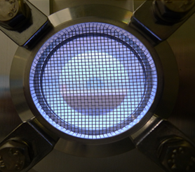
It is a chemical process used to produce high quality, high-performance, solid materials. The process is often used in the semiconductor industry to produce thin films. In typical CVD, the wafer (substrate) is exposed to one or more volatile precursors, which react and/or decompose on the substrate surface to produce the desired deposit.
XPS is a surface spectroscopic technique for quantitative measurements of the elemental composition or stoichiometry and the chemical state of the present elements, like their oxidation state and chemical bonds. XPS is highly surface sensitive, giving chemical and binding energy information from the a narrow region close to the surface.