CVD is a thermal process because a certain thermal energy is needed to decompose the gas precursors and reassemble them in the material to be deposited. Processing conditions in a CVD should avoid gas-phase reactions (homogenous deposition) and should favor that the deposited layer is assembled in the substrate as a surface process (heterogeneous deposition). This can be achieved at atmospheric pressure (APCVD) by heavily diluting the active gases. When these gaseous precursors are let to react in a rarefied the process is termed Low Pressure CVD (LPCVD). The partial vacuum avoids gas-phase reactions. The low pressure also favors larger diffusivity of the species so that an LPCVD process can decorate cavities and led to conformal coatings when a topography is present. The conformality is also spurred by the process temperature which favors movement of the species along the surface. Pressures are usually in the millitorr-torr range and temperatures range from 400-800C (depending on the energy needed to decompose the gas precursors). PECVD is a particular form of CVD that takes place in vacuum but in which a plasma is used to assist the decomposition of the gas precursors. This usually allows lowering the temperature of the process to a few hundred centigrade degrees, which can be run on less temperature resistant substrates or without setting off temperature triggered unwanted processes.
Sample dimension: 1.2mm x 0.6 mm
Sample holder compatible with several other CNR-IOM laboratories (including STM, IPES, BACH beamline)
UHV system (base pressure:~10-10mbar)
The CVD system is directly connected to the following instrumentation, for in situ analysis:
- XPS and UPS analysis chamber, equipped with a conventional X-ray source Mg Ka, He discharge lamp, hemispherical electron energy analyser (120 mm by PSP)
- low energy electron diffraction (LEED)
- supersonic cluster source (AMPHIRO)
- UHV evaporators
- residual gas analyser
- sputter-gun
CSIC-CNM
Spain
Tempress battery of 4 LPCVD tubes
Deposition of LPCVD high quality layers of silicon nitride and polysilicon
Quartz tubes and heaters for LPCVD thermal processes up to 800ºC
Precursors: high purity gases: Silane, DCS, NH3, O2 and N2. TEOS
Wafers of 100mm or 150mm
Isolated chips allowed with restrictions
Substrates with metals or polymers NOT allowed
10 mTorr range base pressure
High temperature up to 600ºC/800ºC
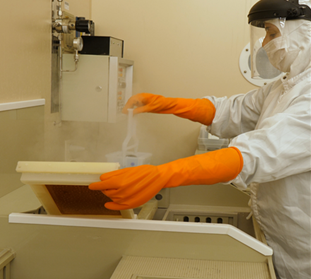
Clean room class 100 ambient
RTA or diffusion furnaces for post-deposition annealing and/or doping
Optical microscope, reflectometer and ellipsometer for film thickness measurement, confocal microscope
Si3N4 deposition around 800ºC and polysilicon deposition between 550ºC - 650ºC. SiO2 deposition at 700ºC
Deposited film thicknesses between 30nm-3 microns for polysilicon and SiO2, and between 30nm-600nm for silicon nitride.
Manual placing in vertical position in a quartz carrier onto an automatic boat loader
Amorphous or semi-amorphous polySi deposition for microsystems applications
Remote
CSIC-CNM
Spain
PECVD AMAT P5000 and Oxford Plasmalab800
Plasma enhanced deposition of SiNx, SiOx and amorphous Si
Passivation
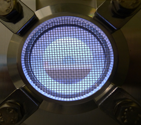
Reaction chambers under vacuum with plasma RF source (13,56MHz) and LF source (Plasmalab: 50-460KHz) for PECVD process below 400ºC
Precursors: Silane, NH3, N2O, H2, TEOS, TMPi, TMB, O2 and N2
Samples and wafers up to 6”
Substrates with polymers NOT allowed
AMAT: substrates with CMOS contaminant metals (alkalines or noble metals) NOT allowed
10 mTorr - 5 Torr range pressure
Temperature range: 200ºC – 430ºC
RTA or diffusion furnaces for post-deposition annealing
Optical microscope, reflectometer and ellipsometer for film thickness measurement, confocal microscope
RF power up to 1,2 kW (Amat)/600W(Plasmalab)
LF power up to 500W(Plasmalab)
Deposited film thicknesses between 30 nm -3 mm for SiOx, between 30 nm -1.5 mm for SiNx and between 30 nm -300 nm for a-Si
Automatic wafer cassette loading
Plasmalab: manual positioning on the bedplate
All in horizontal position
TEOS based SiOx doped with B and P for BPSG or PSG deposition
no
na
na
0
LUND + MAX IV
Sweden
PECVD - MicroSys 200 (706)
Plasma enhanced deposition of SiNx, SiOx, Si
Process gases Ar, SiH4, NH3, N2, O2, NF3, N2O
Up to 4” wafer
Turbomolecular pumping
Deposition at 20-300° C
Deposited film thicknesses typically 20-300nm
ICP-plasma
C2N-CNRS
France
PECVD UNAXIS D200
This PECVD reactor is used for the deposition of common materials such as Silicon oxide or nitride and amorphous silicon. It can be used as well to deposit periodic multi-layers (DBR). No optical monitoring.
Materials: SiO2, Si3N4, a:Si-H
Temperature: 150 °C -280°C
Max sample size: 4 mm height
Max sample size: 8 inches
EURONANOLAB
France
CVD at EURONANOLAB - IEMN
EURONANOLAB
France
CVD at EURONANOLAB - FEMTO-ST
EURONANOLAB
France
CVD at EURONANOLAB - LAAS
EURONANOLAB
France
CVD at EURONANOLAB - PoliFAB
EURONANOLAB
France
CVD at EURONANOLAB - IMM
EURONANOLAB
France
CVD at EURONANOLAB - MMI
na
no
na
na
0
no
EURONANOLAB
France
CVD at EURONANOLAB - IMT
INL
Portugal
FIRST NANO EASY TUBE 3000
Hot-wall quartz-tube furnace for APCVD and LPCVD
Used for deposition of graphene, hexagonal boron nitride, 2D materials, and carbon nanotubes
Substrates up to 10×15 cm
3 temperature zones, with operating temperatures up to 1100°C with an accuracy of ±0.2°C around the setpoint
RIE is used to etch various materials under vacuum in the presence of reactive ions. The sample to be etched is placed in a vacuum chamber and gas is injected into the process chamber via a gas inlet in the top electrode. The lower electrode is negatively biased and a single RF plasma source determines both the ion density and their energy.
Ultraviolet lithography also known as optical or photolithography is the most commonly used patterning technique in microfabrication. A photosensitive material (photoresist) is spin-coated onto the substrate to be patterned. The photoresist is illuminated with UV light through a photomask which contains the relevant geometric patterns.
A set of classical microelectronic processes for pattern transfer through etching of thin films than are co-adjuvant to the functional materials of a given sytem under study in the micro or nano domain. It includes wet and dry etching of all those ancillary dielecric or conducting materials.
A set of classical microelectronic processes for deposition, of ancillary materials that are co-adjuvant to the obtention in the micro or nano domain of the functional materials that are the object of the Growth and Synthesis installation. It includes LPCVD and PECVD layers deposition or deposition of metal layers by PVD.
In SEM a beam is scanned over a sample surface while a signal from secondary or back-scattered electrons is recorded. SEM is used to image an area of the sample with nanometric resolution, and also to measure its composition, crystallographic phase distribution and local texture.