Micro-fabrication
UVL Ultra Violet Lithography

Ultraviolet lithography also known as optical or photolithography is the most commonly used patterning technique in microfabrication. A photosensitive material (photoresist) is spin-coated onto the substrate to be patterned. The photoresist is illuminated with UV light through a photomask which contains the relevant geometric patterns.
UV-SL UV-Soft lithography
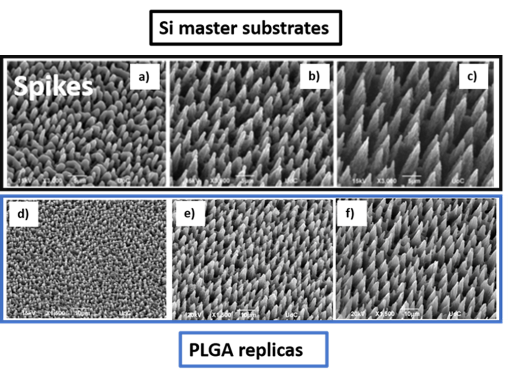
Soft Lithography has been successfully used to transfer well-defined micro sized patterns from rigid materials to surfaces of soft materials and biomaterials eg natural or synthetic polymers, allowing the replication of high fidelity microenvironments at low cost and with great repeatability.
DWL Direct write lithography
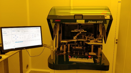
Direct Writing lithography (DWL) is a Maskless lithography technique in which the pattern is transferred directly onto the surface of the wafer without the need of a photomask. A direct laser writer, guided by a control computer, “writes” the patterns that conform one layout level directly onto the resist-covered substrates.
I&GLS I & g-line steppers

Geometric patterns in a photo-mask are transferred to a substrate. Mask aligners project in a single UV shot the full wafer design. Steppers project a single chip onto the substrate in a step and repeat sequence. Resolutions (0.5um) and better local alignment with previous patterns are achieved. Max chip size 1.5-2.2 cm. Full wafers only.
II Ion implantation

It is the kinetic insertion of electromagnetically accelerated ions into substrates to change the physical, chemical, or electrical properties of the sample. It is one of the ways how extra dopants are introduced in silicon substrates. Different elements such as B, P, As, Si, N, H, Ar, Ge, Mg, Al, Cl can be implanted. Small pieces can be processed.
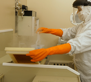
SOTP Silicon oxidation and thermal processes
Processes involving exposure of samples to oxidizing or inert ambient at high temperature (300- 1150C). Tubular diffusion furnaces are used for the growth of an SiO2 layer on silicon (as a dielectric or etching/implant hard mask), densification annealing of other layers, metal sintering processes or thermal activation or diffusion of impurities.
Standard depos. Standard chemical and physical deposition cleanroom/lab processes
A set of classical microelectronic processes for deposition, of ancillary materials that are co-adjuvant to the obtention in the micro or nano domain of the functional materials that are the object of the Growth and Synthesis installation. It includes LPCVD and PECVD layers deposition or deposition of metal layers by PVD.
Standard etching Standard dry/wet patterning cleanroom/lab processes
A set of classical microelectronic processes for pattern transfer through etching of thin films than are co-adjuvant to the functional materials of a given sytem under study in the micro or nano domain. It includes wet and dry etching of all those ancillary dielecric or conducting materials.
ECD Electrochemical deposition

A metal coating to a metallic or another conducting surface can be applied by means of an electrochemical process. A current is passed from an anode to a cathode through an electrolyte causing the dissociated metal ions to gain electrons and oxidize on the surface of the cathode (surface to be coated), thereby forming a metallic coating.
CD&P Chip dicing & packaging

When components must be tested or used singularly, it provides the device with a mechanical body, environment protection, thermal heat sinking and electrical connection to the real world. It encompasses dicing individual dies with automatic diamond saws and chip-to-package wire bonding (wedge, bond and ribbon).
PSN Plasma Surface Nanostructuring

Plasma processing technique that allows for simultaneous chemical AND topographical modification of polymeric surfaces producing micro and nanotexturing variable in height and density. This nanoroughness in combination with chemical modification may lead to superhydrophilic or superhydrophobic surfaces.

