UV-Soft lithography

Nano to Micro/Macro (Micro-fabrication)

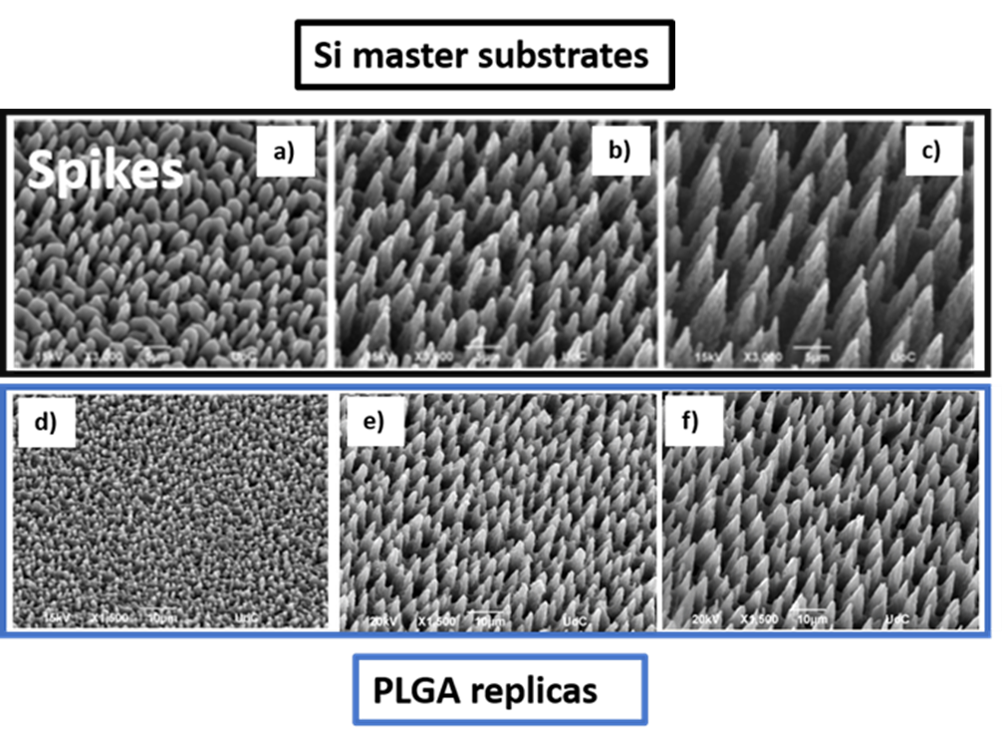
Soft lithography is used to fabricate substrates with surface topographies and structures at the nano- and micro-meter scale with high fidelity, repeatability and at low cost. Generally, it has been successfully used to transfer well-defined micro sized patterns from silicon or stainless-steel masters to surfaces of soft materials and biomaterials eg natural or synthetic polymers, allowing the replication of controlled microenvironments.  The principle behind Soft Lithography: an elastomeric stamp or mold is the key element that transfers the pattern to the soft substrate and flexible organic molecules and materials are used.

Soft lithography is used to produce well defined micro and nano-sized patterns such as microcones, ripples, grooves etc from a master substrate to an elastomer mold (negative replica). Master substrates are usually very stiff and rigid, so the role of the elastomer is to be separate of the master and polymeric replica. Poly(dimethylsiloxane) (PDMS) is the most widely used elastomer mold because it has excellent properties, such as excellent flexibility, optical transparency, chemical resistance, durability, ease of release/peeling off, reversible deforming properties, and low cost.


i
@
          provided at NFFA-Europe laboratories by:
CNR-IOM @TS
Italy
FORTH
Greece
EURONANOLAB
France
i
@
          provided at NFFA-Europe laboratories by:
CNR-IOM @TS
Italy
FORTH
Greece
EURONANOLAB
France

Also consider

Nano to Micro/Macro

Standard depos. Standard chemical and physical deposition cleanroom/lab processes

A set of classical microelectronic processes for deposition, of ancillary materials that are co-adjuvant to the obtention in the micro or nano domain of the functional materials that are the object of the Growth and Synthesis installation. It includes LPCVD and PECVD layers deposition or deposition of metal layers by PVD.

Nano to Micro/Macro

Standard etching Standard dry/wet patterning cleanroom/lab processes

A set of classical microelectronic processes for pattern transfer through etching of thin films than are co-adjuvant to the functional materials of a given sytem under study in the micro or nano domain. It includes wet and dry etching of all those ancillary dielecric or conducting materials.

Lithography & Patterning

RIE Reactive Ion Etching

RIE is used to etch various materials under vacuum in the presence of reactive ions. The sample to be etched is placed in a vacuum chamber and gas is injected into the process chamber via a gas inlet in the top electrode. The lower electrode is negatively biased and a single RF plasma source determines both the ion density and their energy.

Electronic & Chemical & Magnetic Characterization

MFDC Magnetic/ferroelectric/dielectric char.

We provide modular experimental stations to study the evolution of electric and magnetic dipole orders, and their degree of coupling, which is an identifying feature of novel magneto-electric systems. Features for designing multifunctional devices, such as magneto-electric sensors or high-capacity four-state logic memories, can be assessed.

Structural & Morphology Characterization

SEM Scanning Electron Microscopy

In SEM a beam is scanned over a sample surface while a signal from secondary or back-scattered electrons is recorded. SEM is used to image an area of the sample with nanometric resolution, and also to measure its composition, crystallographic phase distribution and local texture.