Direct write lithography
Nano to Micro/Macro (Micro-fabrication)
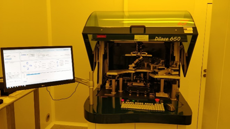
In front of or additionally to traditional photolithography, where the use of a photomask and a mask aligner tool or a reticle and a stepper are needed to transfer the designed layouts onto the substrates via a photosensitive resist coating, Direct Writing Lithography constitutes another photolithography technique which provides a fast and versatile technology especially suited for its use in R+D or in the prototyping stages.
In this technology, Direct laser writers are used in nsubstitution of traditional mask aligners or even steppers to directly expose the photoresist that is covering the surface of the substrates, being controlled by a software which reads the patterns in the designed layout (for instance GDS files) and guides a deflector to reproduce the patterns onto the resist.
Some tools can combine two approaches of photoresist exposition: the rasterized approach, for larger patterns, and the vectorial direct writing approach, where the radiation is focused to a narrow beam that is scanned in vector form across the resist, which allows the best resolution at the cost of lowering the exposition speed.
Noticeably, a key advantage of maskless lithography is the ability to change lithography patterns from one run to the next, avoiding incurring in most of the costs of generating a new photomask, both in economical and time terms
Instruments datasheets
Also consider
EBE e-beam evaporation
RIE Reactive Ion Etching

SEM Scanning Electron Microscopy

UVL Ultra Violet Lithography

XRM X-Ray Microscopy


