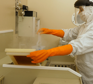
In a good number of occasions, the process for obtaining a layer under study conveniently patterned, isolated, ready to be transferred, or to be contacted needs for a set of ancillary materials that, despite not being the object of the scientific interest, are of crucial importance as they not only make possible the preparation and obtention of the main layers, but also can condition some of their basic properties.
This set of techniques contains the required suite of pattern transfer and/or etching processes for such ancillary materials, such as silicon nitride, silicon oxide, polysilicon that can be used as etching masks, implantation and diffusion barriers, dielectric barriers, spacers or conductive layers. Those materials can be etched and patterned by chemical wet etching or by Reactive Ion Etching (RIE) using appropriate masks, or making use of lift-off process. Those materials can be used themselves as etching masks (for instance in the case of Al layers for deep RIE patterning of substrates), or as adhesion or barrier layers or directly as layers for providing the required electrical contact.
A set of classical microelectronic processes for deposition, of ancillary materials that are co-adjuvant to the obtention in the micro or nano domain of the functional materials that are the object of the Growth and Synthesis installation. It includes LPCVD and PECVD layers deposition or deposition of metal layers by PVD.
RIE is used to etch various materials under vacuum in the presence of reactive ions. The sample to be etched is placed in a vacuum chamber and gas is injected into the process chamber via a gas inlet in the top electrode. The lower electrode is negatively biased and a single RF plasma source determines both the ion density and their energy.
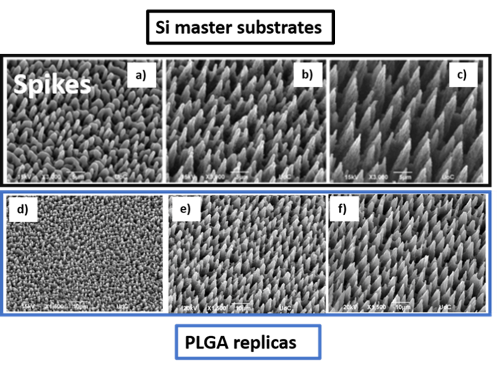
Soft Lithography has been successfully used to transfer well-defined micro sized patterns from rigid materials to surfaces of soft materials and biomaterials eg natural or synthetic polymers, allowing the replication of high fidelity microenvironments at low cost and with great repeatability.
In SEM a beam is scanned over a sample surface while a signal from secondary or back-scattered electrons is recorded. SEM is used to image an area of the sample with nanometric resolution, and also to measure its composition, crystallographic phase distribution and local texture.
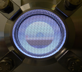
E-Beam evaporation is a physical vapor deposition (PVD) technique whereby an intense electron beam is generated from a filament and steered via electric and magnetic fields to strike the source material (e.g. pellets of Au) and vaporize it within a vacuum environment.