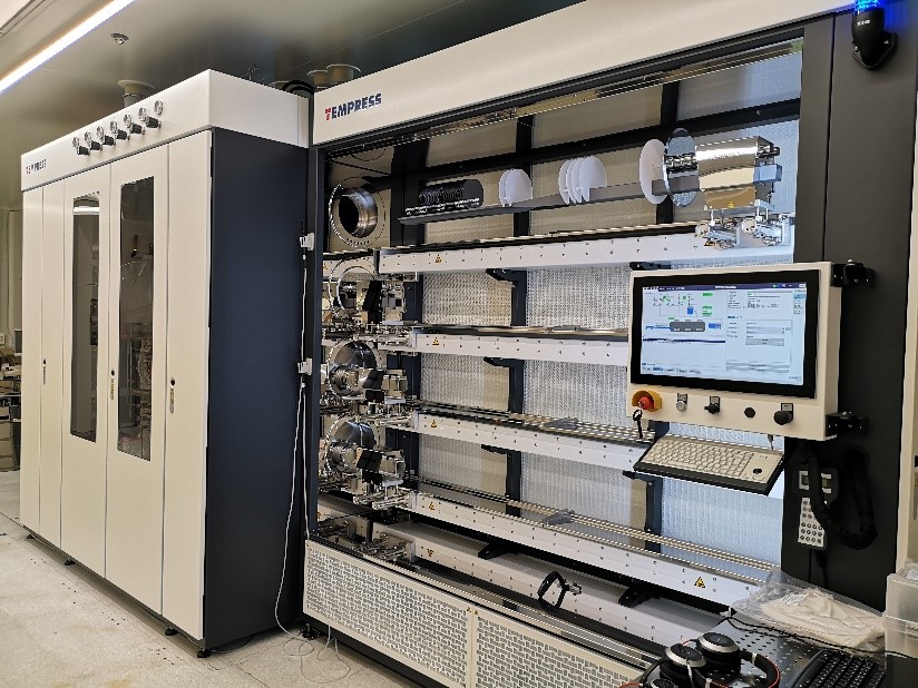
Silicon oxidation and thermal processes
Nano to Micro/Macro (Micro-fabrication)
By combining high temperature and gas injections, it’s possible to modify the physical, optical or electrical properties of materials. For example, O2 or H2O ambient are used to grow silicon dioxide on Si. Inert ambient (N2, Ar)is used to densify layers or to activate and redistribute dopant impurities introduced previously by ion implantation. N2/H2 is used for aluminum sintering.
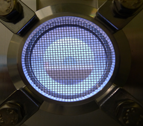
Silicon Oxidation: is the exposure of silicon (or polysilicon) to the action of gas oxidants (O2- termed dry oxidation, H2O – termed wet oxidation) at high temperatures (800-1150C). Part of the silicon of the surface (layer) is consumed and transformed in SiO2 so the starting thickness of the silicon layer is reduced (roughly 50% of the thickness of the obtained silicon dioxide); it can be used for thinning silicon micro-nanostructures. SiO2 layers can be ancillary used to interpose a dielectric barrier or as an etching or implanting mask.
Annealing processes: An annealing is a thermal process in which the substrates are exposed to different temperatures, times and environments depending on the pursued objective such as the post-implant annealing for impurities activation, the fluidization of interlevel dielectric layers, annealing of aluminum layers for contacts formation and the densification of different deposited layers
Instruments datasheets
Also consider
RIE Reactive Ion Etching

XPS X-ray Photoelectron Spectroscopy

UVL Ultra Violet Lithography

Standard depos. Standard chemical and physical deposition cleanroom/lab processes
SEM Scanning Electron Microscopy


