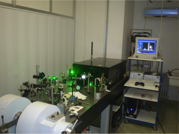
AFM is a surface sensitive technique permitting to obtain a microscopic image of the topography of a material surface. Typical lateral image sizes are within a range of only a few Nanometers to several 10 Micrometers, whereas height changes of less than a Nanometer may be resolved.
A fine tip attached to a cantilever is scanned across the material surface and enables to measure height changes via a laser that is reflected from the rear side of the cantilever onto a segmented photodiode. The position of a laser spot on the photodiode permits to track height changes as e.g. due to a nano-particle on the surface or an atomic terrace of a single crystal surface. A feedback loop controls the tip-surface distance and therefore ensures stable imaging conditions.
Different operation modes like contact or non-contact mode can be used to optimize the imaging conditions with highest lateral resolution on one hand and least sample interaction on the other hand.
Additional surface properties may be obtained for each point of the scan like friction force by lateral force imaging and magnetization properties by magnetic force imaging. Elasticity maps of heterogeneous sample surfaces can be obtained by non-contact phase imaging utilizing the phase shift arising from the local penetration behaviour of the tip into the surface.
Surface topography of hard or soft samples
Acquisition in Tapping or Peak Force Tapping modes
Bruker Dimension Icon/Fast Scan
Optical microscope to visualize sample: 5 Mpixel digital camera; 180 µm to 1465 µm viewing area; digital zoom and motorized focus
spatial resolution < 10 nm
Height resolution around 0.1 nm
Typical X-Y scan range of 90 µm by 90 µm, Z range of 10 µm (Z sensor noise level < 50 pm in closed-loop)
Motorized position stage (X-Y axis) 180 mm × 150 mm (< 3 µm repeatability)
From a few mm2 to 200 mm wafer
Air or controlled atmosphere (AFM inside a glove box with N2 : level of O2 and H2O around ppm)
Surface potential mapping by Kelvin probe force microscopy (KPFM)
Dopant mapping by scanning capacitance microscopy (SCM) or scanning spreading resistance microscopy (SSRM)
Mechanical information by force curve analysis (Peak Force quantitative nanomechanics, Force volume, nano-indentation)
Heater-cooler (-30 to 200 °C)
CEA/LETI
France
UHV AFM
Surface topography of samples
Acquisition in non-contact mode
Omicron/ AFM VT-XA
Optical microscope to visualize sample: 5 Mpixel digital camera; manual zoom and focus
Spatial resolution < 10 nm
Height resolution around 0.1 nm
Typical X-Y scan range of 8 µm by 8 µm, Z range of 3 µm
Motorized position stage (X-Y axis) 10 mm × 10 mm
10 x 10 mm2 maximum
Ultra-High Vacuum (10-10 mbar)
Surface potential mapping by Kelvin probe force microscopy (KPFM)
Surface photo-voltage measurement with visible sources (red, green and blue)
Analysis at variable temperature (50 to 500 K)
Ar sputtering for surface cleaning
Sample heating up to 1000K. LEED
Auger spectroscopy
Sample transfer through vessel or UHV suitcase
DESY + PETRA III
Germany
AFM @ DESY NanoLab
Topographic imaging of surfaces
AFM contact and tapping mode, STM tunnelling spectroscopy, Lateral force mode
CP-II instrument from Digital Instruments
Optical microscope for laser and sample alignment
Sub-atomic resolution in x, y, z by piezo scanner
Large area scanner (90 µm)
High resolution scanner (5 µm)
Sample size: 10 mm x 10 mm
Ambient room temperature and pressure
JCNS @MLZ
Germany
AFM
Surface topography of hard and soft samples, acquisition in tapping or contact mode, magnetic force microscopy
Keysight Technologies N9414A Series 5500 microscope
Optical microscope for laser and sample alignment
Spatial resolution < 10 nm
Height resolution around 0.5 nm
X-Y scan range of max. 90 µm by 90 µm, Z range of 7 µm
Noise level <5Å in XY, <0.5Å in Z
From a few mm2 to 20x20 mm2
Ambient pressure, room temperature
LUND + MAX IV
Sweden
AFM: Bruker Icon
Surface topography
Tapping mode and PeakForce Tapping (PFT)
Angstrom resolution in vertical direction, nm resolution in in-plane, depends on cantilever
Solid sample, wafer up to 8" diameter or smaller pieces, max a few mm thick
Ambient
Optical system: 410-1845X magnification range, color video camera, motorized zoom system
No
PSI
Switzerland
Surface Science Lab @ Laboratory for Micro- and Nanotechnology
Surface topography of hard and soft samples, by tapping and contact scanning modes
lateral resolution < 10 nm, height resolution around 1 nm
X-Y scan range of max. 50 µm by 50 µm, Z range of 3 µm
From a few mm2 to 20x20 mm2
Air
Digital camera, digital zoom
CNR-IOM @TS
Italy
Asylum
Surface topography of hard and soft samples, acquisition in tapping or contact mode, in ambient conditions or liquid environment, Force curves on cells and tissues, Force Mapping Mode (force volume), Nanolithography, Nanomanipulation, Magnetic Force Microscopy
MFP-3D Bio Asylum Research/Oxford Instruments
Top view optics for opaque samples and for laser alignment; Inverted microscope available for transparent supports (glass slides, petri dishes): possibility of epifluorescence measurements
Spatial resolution < 10 nm Height resolution around 0.2 nm
X-Y scan range of max. 90 µm by 90 µm, Z range of 12 µm Noise level <5Å in XY, <0.5Å in Z
From a few mm2 to 10x10 mm2 for measurements in liquid. Up to 10 cm x 4 cm for measurements in air
Ambient temperature for in air measurements; possibility of temperature control 0°C - 60°C in a liquid cell for 1x1 cm2 samples
no
na
no
na
0
CIC biomaGUNE
Spain
Multimode V from Bruker
EURONANOLAB
France
AFM at EURONANOLAB - CEITEC
EURONANOLAB
France
AFM at EURONANOLAB - MMI
na
no
na
no
na
0
EURONANOLAB
France
AFM at EURONANOLAB - IMT
KIT
Germany
AFM at KIT
Measurement under ambient condition or with Nitrogen atmosphere, for specific applications measurements in liquid are available. Due to clean room location and very massive building, a extremely low noise level is attained to enable sub nm z resolution. Maximum size of a single scan is about 100 by 100µm. this is rarely done as this takes hours to do.
Typical samples are a few mm small and mounted on a carrier to protect the sample and to ease handling. If you consider AFM as a suited technology be aware that the total height variation of your Region of Interest RoI must be less than 5µm including surface roughness, tilt and waviness.
na
Detection is done via a mechanical lever made from Si or SiN. For micro indentation a steel cantilever is used. Typical size of a cantilever is a fraction of a human hair diameter. So its delicate but on the other hand very sensitive so that forces in the nN range can easily be detected.
Depending on the Cantilever tip radius, a lateral resolution of <1nm is attained. With cantilever of a suited geometry, the z resolution is in the range of 0,3nm depending on some parameters that have to be discussed
As mentioned the scan size is approximately 100 by 100µm. Typical scans are up to 20 by 20µm. With sufficient resolution to be superior to optical metrology, a point density of >10points per µm is required. to make full use, a point density of >100points per µm is desirable. That makes single measurements slow. Guess is something like 30 minutes per scan for medium resolution and >60 minutes for HR scans. Positioning is sub µm precise if suited markers are within the scan range.
Sample can be anything that is flat and at least semi rigid. Gels can be measured, grease with some limitations, and nano particle dust only if the particles adhere to the sample holder. At least if they are fixed. Samples with real 3D surfaces like parabolic mirrors or grids with lenses need to be checked for accessibility. We have some experience in how to mount samples. and for subsequent measurements we offer a carrier system to interchange samples.
We do not have a vacuum chamber. The lab provides ambient condition with humidity and temperature continuously monitored. We have a heater/cooler stage that allows to cool down to -25 °C and to heat up to 250°C with a nitrogen air flow to avoid oxidization or condensing water on the surface.
In addition to standard AFM modes, we offer PF-Tapping, PF-KPFM, modes for adhesion measurements and a specific setup to monitor the tip-sample interaction with an additional camera generating movies of the cantilever while in interaction with the surface. This is a valuable source of additional information especially for particle particle or particle fiber interaction analysis.
As we have s automation Software installed, even long time measurements can be performed.
AFM measurements are supported by a confocal scanning microscope and a vertical scanning interferometer to generate a more realistic impression of the region of interest. Typically, only if these instruments show that the surface is homogeneous, then the AFM information gained from a very small scan is representing the sample at all.
na
na
na
CNR-DSCTM
Italy
AFM
mesurements of topological features
EURONANOLAB
France
AFM at EURONANOLAB - IEMN
EURONANOLAB
France
AFM at EURONANOLAB - LAAS
EURONANOLAB
France
AFM at EURONANOLAB - FBK
EURONANOLAB
France
AFM at EURONANOLAB - PoliFAB
EURONANOLAB
France
AFM at EURONANOLAB - CNR-Nanotec
CSIC-ICMAB
Spain
Keysight 5100 AFM
Keysight 5100 AFM comprises a scanner of 60 x 60 microns in X / Y and 6 microns in the Z axis. The equipment can use a special liquid cell and controlled environment chamber for conducting scanners at low humidity or in nitrogen. The maximum sample size is 3x3 cm in X / Y and 2 cm thick. The equipment works in the Constant Amplitude Dynamic mode for obtaining topographic images, however Contact mode is also a possibility. The equipment uses an external generator module that can apply in-plane magnetic fields upto + -800 Oe. The equipment is specifically employed to acquired topographic images, having a low noise architecture that allow the acquisition of 500 nm size images.
x, y positioning
na
no
na
0
CSIC-ICMAB
Spain
Keysight 5500 AFM
Keysight 5500, it has a 90x90 microns in X / Y and 15 microns in the Z axis closed loop scanner. The SPM is equipped with three independent Lock-in amplifiers that can be fully configured through the use of an external Signal Access Box. The equipment can be used with the following modes: Piezoresponse Force Microscopy, Bimodal Atomic Force Microscopy and Dynamic Topography. It also has aClosed Loop capability that significantly improves the positioning in X and Y. Sample size is limited to 3 x 3 cm in the X and Y directions and 1 cm in the Z direction. A Q-Control is also available to enhance images in liquid. It has a separate accessory for measuring humidity and temperature inside SPM box. A separate heater up to 350ºC can be used in this equipment.
na
no
na
0
CSIC-ICMAB
Spain
Keysight 5500 LS AFM
Keysight 5500 LS, it has a 90x90 microns in X / Y and 15 microns in the Z axis closed loop scanner. The SPM is equipped with three independent Lock-in amplifiers that can be fully configured through the use of an external Signal Access Box. The equipment can be used with the following modes: Piezoresponse Force Microscopy, Electrostatic Force Microscopy, Kelvin Probe Force Microscopy, Scanning thermal Microscopy (from 2Q2016), Current Sensing Atomic Force Microscopy, PhotoConductive Atomic Force Microscopy, Bimodal Atomic Force Microscopy. It also has Closed Loop capability that significantly improves the positioning in X and Y as well as a motorized stage, with accuracy of + -3 microns, and a range of + -15cm in X / Y and 3cm in Z axis, so sample size may reach up to 25 x 25 cm and 3 cm thick. A Q-Control is also available to enhance images in liquid. It has a separate accessory for measuring humidity and temperature inside SPM box. A sample cooler and heater with a range of -60ºC to 90ºC and a separate heater up to 350ºC can be used in this equipment. A special current-to-voltage amplifier "Resiscope II" from CSI instruments can be used to acquire topography images. A separate accessory for illuminating samples in the Visible and UV spectra is also available.
SPM3: Keysight 5500 AFM (aka Luke)
Keysight 5500, it has a 90x90 microns in X / Y and 15 microns in the Z axis closed loop scanner. The SPM is equipped with three independent Lock-in amplifiers that can be fully configured through the use of an external Signal Access Box. The equipment can be used with the following modes: Piezoresponse Force Microscopy, Bimodal Atomic Force Microscopy and Dynamic Topography. It also has aClosed Loop capability that significantly improves the positioning in X and Y. Sample size is limited to 3 x 3 cm in the X and Y directions and 1 cm in the Z direction. A Q-Control is also available to enhance images in liquid. It has a separate accessory for measuring humidity and temperature inside SPM box. A separate heater up to 350ºC can be used in this equipment.
na
no
na
0
UMIL
Italy
Bioscope Catalyst AFM (Bruker)
Statistical analysis of surface morphology of thin films and nanostructures; Metrology of nanometer-sized objects (proteins and nanoparticles); Nanotribological and nanomechanical characterization of (bio)interfaces; Force-spectroscopy; Scanning electric impedance microscopy; Calibration of AFM probes.
na
no
na
0
CSIC-ICMAB
Spain
NX10 - Park Systems
Contact mode
Tapping mode
Non-contact mode
Friction Force Microscopy (FFM)
Electrostatic Force Microscopy (EFM)
Kelvin Probe Microscopy (KPFM)
Piezoresponse Force Microscopy (PFM)
Nanomechanical properties characterization
Magnetic Force Microscopy (MFM)
Ups to 10 nm in XY and 0.05 nm in Z. Dependent of sample type and conditions.
Maximun scan range 100 µm x 100 µm in XY, few µm in Z.
Capability of performing consecutive scans an stitch them afterwards.
Ups to 100 mm x 100mm samples on XY and around 20 mm on thickness.
In SEM a beam is scanned over a sample surface while a signal from secondary or back-scattered electrons is recorded. SEM is used to image an area of the sample with nanometric resolution, and also to measure its composition, crystallographic phase distribution and local texture.
Brillouin spectroscopy is an empirical spectroscopy technique which allows the determination of elastic moduli of materials. The technique uses inelastic scattering of light when it encounters acoustic phonons in a crystal, a process known as Brillouin scattering, to determine phonon energies and therefore interatomic potentials of a material.
XPS is a surface spectroscopic technique for quantitative measurements of the elemental composition or stoichiometry and the chemical state of the present elements, like their oxidation state and chemical bonds. XPS is highly surface sensitive, giving chemical and binding energy information from the a narrow region close to the surface.
In TEM/Scanning TEM (STEM) high energy electrons incident on ultra-thin samples, allow imaging, diffraction, electron energy loss spectroscopy and chemical analysis of solid materials with a spatial resolution on the order of 1-2 Å. Samples must have a thickness of a few tens of nanometres and are prepared in sample preparation laboratory.
Electron-beam lithography is a direct write nanopatterning technique utilizing a finely focused electron beam in order to write nanoscale patterns on special e-beam resists in two and three dimensions. Compared to other nanostructuring methods, it stands out for its high level of flexibility and resolution and reasonable patterning speed.