Due to the upcoming SLS 2.0 upgrade this technique will be unavailable at PSI until further notice.
Due to the upcoming ELETTRA 2.0 upgrade, this technique will be provided at CNR-IOM(TS) only at laboratories until further notice.
XPS is a surface spectroscopic technique for quantitative measurements of the elemental composition or stoichiometry and the chemical state of the present elements, like their oxidation state and chemical bonds. Due to the limited free path-length of the excited photoelectrons within the material, XPS is highly surface sensitive, giving chemical and binding energy information from the narrow region close to the surface.
Angular resolved (AR) XPS permits to obtain a depth profile of the elemental composition and chemical state in this narrow surface region, and permits to determine the relative concentrations of surface elements versus buried ones, as, e.g., between head and tail groups of adsorbed alkanes. In combination with sputtering, a larger depth profile is possible. The X-ray spot-size on the sample surface is typically in the range of 5-100 µm.
Conventional X-ray source (Mg Kα), He discharge lamp
Mg Ka hv: 1253.6eV; He discharge lamp (hv: 21.2eV, hv: 40.2eV)
PSP 120mm hemispherical electron energy analyser
~0.8eV for XPS, 50meV for UPS
T range: RT-1500°C
Preparation chamber with CVD and PECVD growth facilities, UHV evaporators, LEED, sputter gun, RGA
CNR-IOM @TS
Italy
ARPES, XPS - BACH Beamline @ Elettra Synchrotron
Soft x-ray - VUV and resonant angle-resolved photoelectron spectroscopy, resonant photoelectron diffraction, resonant x-ray photoemission spectroscopy, fast photoemission with selectable polarization;
core levels, valence band, work function, Auger, surface and bulk band dispersion, empty states in the conduction band, magnetic remanence, strain in thin films, time-resolved spectral evolutions during surface reactions
Elettra synchrotron, Apple II undulators; variable polarization (horizontal, vertical, circular ±); beam size on the sample 350x350 (HxV, µm2); vertical size can be reduced on request; flux on sample @ 10µm slits (best resolution) (ph./s) 2x10¹²-6x10¹⁰
35-1650 eV
VG Scienta R3000 analyzer with slit(s) perpendicular to the scattering plane
(E/dE) 20000-5000
Many samples can be acccomodated in a 25x25mm2 area; T range: 50-1200 K (PID-controlled)
XAS is possible in the same chamber; quick XPS acquisition mode (300 ms per spectrum); 4 degree-of-freedom manipulator (rotation axis perpendicular to the scattering plane); possibility to measure at T>300 K; electrical insulation of the sample: possibility to apply a voltage and measure the work function; possibility to superimpose synchrotron beam to external light sources to study photoinduced phenomena
Both preparation and main chambers with heating stages (e-beam, direct current, PBN), ion gun (VG), 4 evaporator ports (CF40), gas inlet valve (variable leak valve), diamond file scraper, cleaver, evaporators for organic molecules, e-beam evaporators (Omicron) for metals (evaporation at low sample temperatures is also possible), LEED (OciLEED)
Base pressure: UHV
CEA/LETI
France
PHI 5000/VersaProbe II
X-ray Photoelectron Spectroscopy micro-analysis of thin-films, bulk materials and prototypical devices
Depth-profiling of inorganic and organic samples
XPS imaging of heterogeneous surfaces at the 10 microns scale
Excitation source: Monochromated X-rays AlKa1
Sputtering source: Monoatomic Ar (0.25-5 keV)
Gas Cluster Ion Source (Ar cluster size 500-2500; primary energies 0.5-20 keV)
X-rays: 1486.6 eV
Multi-channel detection (128)
Energy resolution: > 0.5 eV
Chemical state mapping: > 7 µm lateral resolution at > 0.8 eV energy resolution
5x5 mm² < size < 60 mm diameter
UHV or inert atmosphere transfer is possible to the following tools: ScientaOmicron/NanoESCA, Nano Auger, ToF-SIMS and UHV AFM
4-contacts sample holders for in-situ sample biasing
Routine base pressure 8x10⁻¹⁰ mbar, highest allowed pressure 8x10⁻⁶ mbar
n.d.
x, y, z (for positioning the area of interest)
θ tilt (for variable-angle XPS)
Hot/cold sample plate for in-situ cooling (liquid nitrogen) or heating (< 900°C)
Undulator, source brilliance: 1020 ph/s/mm2/mrad2/0.1% bw/100 mA, polarization available: circular (variable linear hor./vert. in future)
Energy range 250 eV – 3 keV (design), 250 eV – 2.2 keV (at present)
Beamline energy resolution <10 meV at 335 eV, <100 meV at 1 keV
Sample type: solid or gas phase (UHV compatible), angle of incidence light – sample: 0 to 90, spot size ON SAMPLE: 5000 μm x 2000 μm to 10 μm x10 μm (h x v), maximum flux ON SAMPLE: > 1015 ph/s @ 1keV
Techniques available: experimental platform (6 user setups available for collaborations)
designed and built at DESY
no
no
hdf5,tiff
10000
ICN2
Spain
XPS Phoibos 150 (SPECS)
XPS, UPS
- SPECS XR 50 M X-ray source for FOCUS 500 X-ray monochromator with Aluminium (1486.74eV) and Silver (2984 eV)
- SPECS UVS 300 UV light with monochromator with He I (21.2 eV) and He II (40.8eV)
0-1486eV with Al and 0-2900eV with Ag
SPECS PHOIBIOS-150 analyser
0.5eV with Al and 0.5meV with He I
T down to 80K, heating to 700K
Preparation chamber equipped with heating stage (e beam), sputter gun, load lock, LEED, gas inlet leak valve and 3 evaporation ports
Analysis chamber equipped with flood gun to neutralise charging on non conductive samples
UHV
PSI
Switzerland
XPS - Surface Science Lab @ Laboratory for Micro- and Nanotechnology
Sample analysis with micro/spectro-scopy correlation (XPS, UPS, LEED, STM)
SPECS XR 50 M X-ray source for FOCUS 500 X-ray monochromator
Single wavelength, Al Kα, 1486.7 eV
SPECS PHOIBIOS-150 analyser
50K-500K, typically 1cm2, other possibilities to be discussed
Only for standard measurements. Will be decided by the instrument scientists.
No
KE: 0 - 3500 eV
Uni-NG
Slovenia
CITIUS 3
XPS
Al K alpha monochromatized
1486 eV
Scienta R3000 electron energy spectrometer
400 meV
400 micron spot size
Max sample size 8x8 mm, thickness 2 mm, mounted on flag style sample plates (Mo or Cu).
Cryogenic manipulator 5 degrees of freedom (x,y,z, polar angle and tilt), down to 20 K
UPS, trARPES
SEM, TEM
chemical laboratory
Sample heating stage up to 1000 degrees by electronic bombardment
Ar ion sputtering
In vacuum cleaver
Ultrahigh vacuum
LEED, microbalance
(0-1500) eV
CNR-IOM @TS
Italy
XPS@ MBE Lab
Microspot Al Kα conventional source
0.9 eV
1 mm
PSI
Switzerland
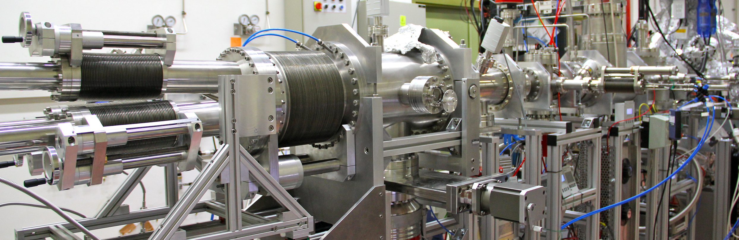
XPS - PEARL Beamline @ Swiss Light Source Synchrotron
The PEARL (Photoemission and atomic resolution laboratory) beamline is dedicated to the structural characterisation of local bonding geometry of molecular adsorbates on metal or semiconductor surfaces, of nanostructured surfaces, and of surfaces of complex materials. It is a soft X-ray beamline with an angle-resolved photoelectron spectrometer for angle-scanned and photon energy-scanned X-ray photoelectron diffraction (XPD)
Bending magnet, linear horizontal, partial circular left/right, flux on sample at 1 keV: 2x10¹¹ph/s, spot size: 170μm H x 73μm V, FWHM, 1mm x1mm
Aloisa is a spectroscopic beamline (XPS, XAS, ResonantXPS, PED) dedicated to Surface Science. Systems: single crystals, Self Assembled Monolayers, small molecule adsorbates (poly- and hetero-aromatics), ultra-thin films. Phenomena: on-surface synthesis and modification of molecular adsorbates, charge transfer at hybrid organic-inorganic interfaces, molecular orientation at surfaces.
Insertion Device: - 1.5 m phase shifting Undulator (constant gap): 21 x 7cm periods. - linear polarization. - fully integrated in the acquistion software suite. Monochromator: - type SX-700 (plane mirror-grating) with collimated beam (2x Paraboloidal Mirrors at 0.5˚ grazing incidence). - multiple working curves for optimization of flux, resolution, rejection of higher orders (depending on specific needs). - linear polarization. - fully integrated in the acquistion software suite. - VERY HIGH TRANSMISSION AT CARBON IONIZATION THRESHOLD (40-50%). - Flux at Sample: ~1x10^12 ph/sec from 200 to 1000 eV in working condition (Exit Slits = 20µm). - photon energy resolving power (E/DE): >5000 from 200 to 900 eV in working condition (10^12 ph/sec).
Monochromator energy range: 130-1500 eV. Undulator First Harmonic:130-450 eV at B.E. = 2.0GeV (140-550 eV at B.E. = 2.4GeV)
XAS: partial electron yield by means of a channeltron equipped with a polarizable grid for low energy secondary electrons rejection (NO drain current measurement available). Simultaneous measurement of drain current on refocussing mirror (i0) for flux normalization and absolute energy calibration at the C, N, O K-edge and Fe, Cr L-edge. XPS: homemade hemisperical analyzer (mean radius 66mm); 2xMCP + 2D-DelayLine detector for very high dynamical range (1 MHz); PED: fully rotatable analyzer with small detection angle (<2˚ FWHM); ResPES: undulator, monochromator, manipulator and analyzer movements fully integrated in the acquistion software suite. FULLY AUTOMATED ACQUISITION SOFTWARE (Labview suite).
XPS: - electron energy resolution: 1% Pass Energy (minimum 35 meV) - standard working conditions: 10-30 eV Pass Energy
Photon beam transverse size at sample position (h x w): 30-50 µm x 150 µm.
SOLID samples with polished surface (reflective) for sample alignment (phosphorum plat with TV camera at the end of experimental station for checking the reflected beam. Sample holders (POD) with on-board heating system (radiative or electron bombardment), LN2 cooling, two thermocouples. Sample size: max thickness 3 mm; max width 12-14 mm; min width 4 mm. Minimum temperature: 150 K Max temperature: 1050 K (flash). PID temperature control with programmable ramps. Real time XPS during heating from 150 to 650 K.
Dedicated software (freeware) for data analysis and fittings (XPS, NEXAFS, ResPES 2D maps) based on IgorPro platform.
Standard UHV equipment for sample cleaning and ordering.
UHV experimental chamber (10^-11 mbar); UHV preparation chamber (10^-10 mbar). Praparation chamber in-line between exp. chamber and refocussing mirror (UHV must be recovered before measurements. Manipulator travelling forth and back between exp. and prep. chambers. Max partial pressure for gas dosing 10^-6 mbar. MBE cryovessel (H2O) with four slots for evaporators, shutters and microbalances. Homemade Knudsen cells (two crucibles, either BN or quartz) with inner thermocouple for organic molecules and low vapour tension matyerials (up to 600˚C). Omicron e-beam cells for metal evaporation.
MANIPULATOR: - fully motorized six-degrees of freedom with high resolution (<0.01˚ on three rotations; <0.01mm on three translations). - horizontally mounted (coaxial to the photon beam) for grazing incidence measurements. - rotations and translations fully integrated in the acquisition software suite for surface scanning (to prevent radiation damage). XAS: change of surface orientation with respect to polarization from Transverse Magnetic (p-pol) to Transverse Electric (s-pol) by sample rotation around the photon beam at constant grazing angle. XPS: standard XPS at grazing incidence (4˚) and normal emission for high signal yield; fully rotatable analyzer (zenithal angle: 0˚-100˚) for any surface azimuth (±95˚) and surface orientation w.r.t. polarization; analyzer rotation fully integrated in the acquisition software suite.
RHEED. Microbalances integrated in the MBE system.
Not allowed to Users.
Not allowed to Users
XPS: photoelectron in the 50-1500 eV range
na
EURONANOLAB
France
XPS at EURONANOLAB - MMI
na
na
no
no
na
0
KIT
Germany
XPS at KIT: Soft X-Ray Spectroscopy, Microscopy, and Spectromicroscopy (WERA)
The soft x-ray analytics facility WERA provides a coherent combination of electron spectroscopies and microscopies for studying in detail the chemical (electronic) and magnetic structure of bulk materials, thin films, and micro- and nanostructured objects.
Methods for Electron spectroscopy and spectromicroscopy: XAS, PES (XPS), SXMCD, µ-XAS, µ-PES (±-XAS), µ-SXMCD, topography
Equipment: Three experimental stations at WERA equipped with PEEM, electron energy analyzer, detectors, cryostats, sample preparation chambers, loadlocks, in-vacuo sample transfer etc.
EURONANOLAB
France
XPS at EURONANOLAB - CEITEC
EURONANOLAB
France
XPS at EURONANOLAB - FBK
EURONANOLAB
France
XPS at EURONANOLAB - LTM
EURONANOLAB
France
XPS at EURONANOLAB - PoliFAB
JRC - ISPRA
Italy
XPS
XPS can identify and quantify the elements present on a surface (elemental composition), their chemical states (chemical shift) and their electronic states.
XPS is routinely used to analyse inorganic compounds, metal alloys, semiconductors, polymers, elements, catalysts, glasses, ceramics, paints, papers, inks, woods, plant parts, make-up, teeth, bones, medical implants, bio-materials, coatings, viscous oils, glues, ion-modified materials and many others
Al monochromatic source Ka hv: 1486.6eV; He discharge lamp (hv: 21.2eV, hv: 40.2eV)
PSP 165mm hemispherical electron energy analyser
T range: -150 to 600°C
~0.45eV for XPS, 50meV for UPS
CNR-DSCTM
Italy
XPS at ISOF
CNR-DSCTM
Italy
XPS At ISOF
CIC biomaGUNE
Spain
XPS/UPS – SPECS SAGE HR-100
determining the composition of the most superficial layer of a material, both qualitatively and quantitatively. It also allows to determine the chemical state of the elements present on the surface of a material
AU-ISA
Denmark
XPS - MatLine beamline @ASTRID2
MatLine is dedicated to the electronic properties of surfaces and interfaces on metal, metal oxide and semiconductor, especially of adsorbed molecules on substrates.
Multi-pole wiggler from ASTRID2; Resolving power 200 to 3,500; Typical Flux 1x10¹¹ photons/sec; Spot size: 0.7 mm X 0.7 mm.
20-700 eV, with the possibility up to 1260eV at lower resolution and flux
SPECS PHOIBOS 150 1D-DLD electron analyzer
Temperatures in the range of 110K – 1200K; Non-insulating samples at size less than 12mm X 7mm X 2mm; Possibility of measuring certain type of powders
2 evaporator ports (CF40), installation without break main vacuum; gas inlet; load-lock; auto heating while measuring; LEED; ion gun; RESPED is not available at the moment
In TEM/Scanning TEM (STEM) high energy electrons incident on ultra-thin samples, allow imaging, diffraction, electron energy loss spectroscopy and chemical analysis of solid materials with a spatial resolution on the order of 1-2 Å. Samples must have a thickness of a few tens of nanometres and are prepared in sample preparation laboratory.
XRD provides non-destructive information on the structural order of a material. At large scattering angles XRD permits to identify different crystal phases and to quantify lattice distances and crystalline volume fractions. At low angles of incidence the surface roughness of a single crystal and the thickness of a deposition layer can be obtained.
In SEM a beam is scanned over a sample surface while a signal from secondary or back-scattered electrons is recorded. SEM is used to image an area of the sample with nanometric resolution, and also to measure its composition, crystallographic phase distribution and local texture.
XAS is sensitive to the local bonding environment of the atom absorbing the X-rays, providing information on oxidation states, local orbital symmetry, molecular orientation and chemically selective density of states. It is widely used in molecular and condensed matter physics, material science, engineering, chemistry, earth science and biology.
We offer a multiple ion-cluster source operating in ultra-high vacuum devoted to the fabrication and characterization of highly controlled nanoparticles. They are produced in gas phase with high purity and controlled size, structure and stoichiometry and they can be collected in the desired coverage on arbitrary surfaces for different uses.