Patterning, replication, and sample navigation
ICP Inductively Coupled Plasma

ICP is a reactive ion etching technique, where plasma is generated by means of inductively coupling RF power in the source. The ion energy bombarding the substrate is independently controlled via the applied bias power. This allows for a wide process space to address from anisotropic deep etching to highly chemical or physical processes.
RIE Reactive Ion Etching

RIE is used to etch various materials under vacuum in the presence of reactive ions. The sample to be etched is placed in a vacuum chamber and gas is injected into the process chamber via a gas inlet in the top electrode. The lower electrode is negatively biased and a single RF plasma source determines both the ion density and their energy.
IBM Ion-beam milling
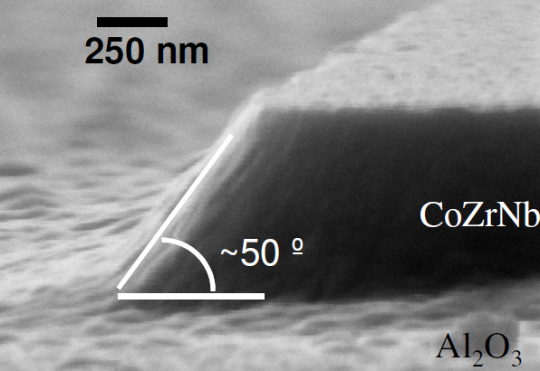
Ion beam milling is a pattern transfer technique used to etch thin films of materials by physical sputtering or milling by use of a broad ion beam. The beam energy, the beam-to-substrate angle as well as the sample rotation speed can be selected for tunable etching conditions according to the application.
NIL NanoImprint Lithography

NIL is a low cost, high resolution and high-throughput method for nanoscale patterning. It creates patterns by mechanical deformation of an imprint resist and subsequent processes. NIL is one of the most promising next generation techniques for large area replication in the nanometer scale. Thermal and UV assisted NIL is possible.
BCL Block copolymer lithography

BCP lithography takes advantage of the self-assembly properties of BCPs to create nanoscale surface patterns in large areas. The main advantages is the process simplicity, the spatial resolution and the high throughput. Block co-polymer patterns are transferred to the substrate by etching using one of the BCP phases as an etching mask.
NOT&P Nano-Object Transfer & Positioning
Nano-Object Transfer & Positioning permits identifying, marking, and transferring pre-selected nano- and microscale single objects and enables their multi-analytical characterization by re-localization with different nano-science instruments at labs and ALFSs.
ALE Atomic Layer Etching
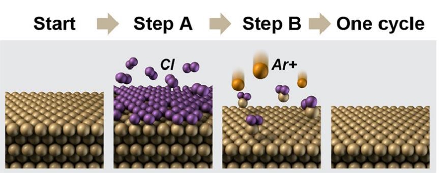
Atomic layer etching is a plasma etching process occurring in cycles of gas dosing and ion bombardment that removes material layer by layer. It has the potential to remove single atomic layers with very low damage. It uses a classical ICP reactor with the additional ability to dose etchant gases and accurately control the ion bombardment energy.

