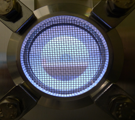
RIE is used to etch various materials under vacuum in the presence of reactive ions. Typically a wide range of materials can be etched by use of various gas mixtures containing fluorine, chlorine, oxygen and other elements. An RF source accelerates stray electrons between a pair of plates in the presence of a low-pressure gas and reactive ions and free radicals (like monoatomic fluorine) are created. The surface to be etched is bombarded by the reactive ions and the material is etched by forming a volatile component. The etching mechanism can either be physical (sputtering mechanism) where the target material is mechanically sputtered away by the accelerated ions, chemical where the ions react with the target material to form a volatile compound, or both. The selection of the etch parameters (gas mixture, gas flow, pressure, RF power and bias) can give control over the anisotropy, selectivity, etching rate, and surface roughness by controlling this etching mechanism.
Power sources ICP 3000W and RIE 600W
System based on fluorinated gases, plasma gases available: SF6, CHF3, C4F8, CF4,Ar,O2,He,N2
Samples sizes up to 8" wafers
Power sources ICP 3000W and RIE 600W
Laser endpoint detection available
Base pressure 3e-7Torr, process pressures up to 100mTorr
Yes
EURONANOLAB
France
RIE at EURONANOLAB - MMI
na
no
no
na
na
0
EURONANOLAB
France
RIE at EURONANOLAB - IMT
C2N-CNRS
France
CCP-RIE NEXTRAL (2)
This Fluorine Reactive-ion etcher (RIE) is dedicated for insulators, semimetals and semiconductor materials (crystalline, glasses and ceramics) .Other applications are dielectric etching mask like SiO2, SiN, resist etching or descum. Moreover metal like W is accepted.
Gas Line: SF6, CHF3, 02
Wafer Holder: 6” to small piece.
Wafers thermalization: 5°C à 40°C.
Mask: electro-and photo-sensible resist, SiO2, Si3N4 / No Metals.
HF generators power: 300 Watt at 13,56 MHz
End point detector: Laser interferometry 670nm
EURONANOLAB
France
RIE at EURONANOLAB - IEMN
EURONANOLAB
France
RIE at EURONANOLAB - FEMTO-ST
EURONANOLAB
France
RIE at EURONANOLAB - LAAS
EURONANOLAB
France
RIE at EURONANOLAB - PoliFAB
EURONANOLAB
France
RIE at EURONANOLAB - IMM
EURONANOLAB
France
RIE at EURONANOLAB - Nanotec
INL
Portugal
SPTS Pegasus
System dedicated for deep reactive ion etching of silicon using the Bosch Process.
Alternating cycles of SF6 plasma etching and C4F8 plasma for polymeric deposition.
A set of classical microelectronic processes for deposition, of ancillary materials that are co-adjuvant to the obtention in the micro or nano domain of the functional materials that are the object of the Growth and Synthesis installation. It includes LPCVD and PECVD layers deposition or deposition of metal layers by PVD.
Ultraviolet lithography also known as optical or photolithography is the most commonly used patterning technique in microfabrication. A photosensitive material (photoresist) is spin-coated onto the substrate to be patterned. The photoresist is illuminated with UV light through a photomask which contains the relevant geometric patterns.
A set of classical microelectronic processes for pattern transfer through etching of thin films than are co-adjuvant to the functional materials of a given sytem under study in the micro or nano domain. It includes wet and dry etching of all those ancillary dielecric or conducting materials.
In SEM a beam is scanned over a sample surface while a signal from secondary or back-scattered electrons is recorded. SEM is used to image an area of the sample with nanometric resolution, and also to measure its composition, crystallographic phase distribution and local texture.
It is a chemical process used to produce high quality, high-performance, solid materials. The process is often used in the semiconductor industry to produce thin films. In typical CVD, the wafer (substrate) is exposed to one or more volatile precursors, which react and/or decompose on the substrate surface to produce the desired deposit.