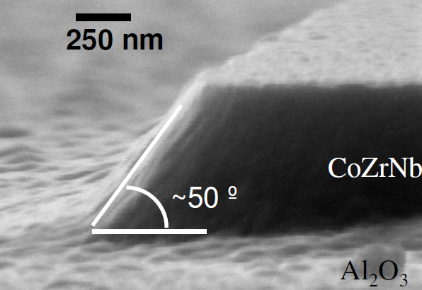
Ion beam milling is performed with a broad beam, RF-excited ion source of relatively large diameter, equipped with an ion accelerator. The highly directional beams of charged particles are directed at a substrate with a predefined hard mask in a high vacuum chamber. A neutralizer is used to neutralize the space charge by providing electrons, assuring optimum etching of dielectric films, not only of metals. To control the etched sidewall profile and to assure radial uniformity during the etching the sample can be tilted with respect to the beam, while it rotates, ensuring axisymmetry. Although the etching rates can be enhanced by use of reactive gases, usually inert gases are used and most materials can be effectively milled with this technique. The technique is highly anisotropic owing to the directionality of the ions. Ion beam milling is the technique of choice for materials that cannot be etched by reactive ion etching or when steep sidewalls are wanted. Typical available gases are Ar, O2, N2, Xe. Often in the same system ion beam deposition of metals and dielectrics can also be performed (typical structures are spin valves and tunnel junctions, passivation layers). Examples of target materials are: NiFe, MnIr, CoFe, Ta, Cu, Al, Ru, NiFeCr, Cr, Ti, Fe, Co, CoFeB, CoZrNb, MnCrPt, Al2O3, Zr, among others. Ion beam deposition can also used for the fabrication of metal oxides by reactive deposition (NiO, CrOx, TiOx, Fe3O4).
@
provided at NFFA-Europe laboratories by:
@
provided at NFFA-Europe laboratories by:
Also consider
Structural & Morphology Characterization
SEM Scanning Electron Microscopy
In SEM a beam is scanned over a sample surface while a signal from secondary or back-scattered electrons is recorded. SEM is used to image an area of the sample with nanometric resolution, and also to measure its composition, crystallographic phase distribution and local texture.
Structural & Morphology Characterization
TEM Transmission Electron Microscopy
In TEM/Scanning TEM (STEM) high energy electrons incident on ultra-thin samples, allow imaging, diffraction, electron energy loss spectroscopy and chemical analysis of solid materials with a spatial resolution on the order of 1-2 Å. Samples must have a thickness of a few tens of nanometres and are prepared in sample preparation laboratory.
Lithography & Patterning
EBL Electron Beam Lithography
Electron-beam lithography is a direct write nanopatterning technique utilizing a finely focused electron beam in order to write nanoscale patterns on special e-beam resists in two and three dimensions. Compared to other nanostructuring methods, it stands out for its high level of flexibility and resolution and reasonable patterning speed.
Growth & Synthesis
MBE Molecular Beam Epitaxy
MBE allows growth of high quality semiconductors, oxides and organic epitaxial layers, with crystal structure commensurate with the substrate. It is used to build nanostructures (quantum dots, nanowires), layered heterostructures for lasers, photodetectors, LED and optoelectronic devices.
Electronic & Chemical & Magnetic Characterization
MFDC Magnetic/ferroelectric/dielectric char.
We provide modular experimental stations to study the evolution of electric and magnetic dipole orders, and their degree of coupling, which is an identifying feature of novel magneto-electric systems. Features for designing multifunctional devices, such as magneto-electric sensors or high-capacity four-state logic memories, can be assessed.