Magnetic/ferroelectric/dielectric char.
Electronic & Chemical & Magnetic Characterization (Magnetic characterisation)
Coupled magnetic and electric phenomena open new avenues in ferroelectric memory devices and sensor technologies. The advanced study of these requires different techniques that are mainly based on capacitor-like geometries.
Our custom-made Magneto-electric workstation consists of a superconducting 7 Tesla magnet, a continuous flow cryostat (liquid-N2 or He operation) and custom-designed probes for use with samples in various forms (polycrystalline pellet, single crystal, film and capacitor topology composites) that altogether provide fully computer-controlled programmable measurements.
Advanced sample environments, with temperature and external stimuli sweeping capabilities, explore the induction of electric polarization (magnetization) by an external magnetic (electric) field.
The infrastructure utilizes a user-friendly LabView programmed interface that fulfills the requirements for characterization of the nanomaterials’ in terms of their dielectric permittivity, in an extended frequency range (50 Hz ≤ f ≤ 2 MHz; option with DC-bias ±40 V) and a broad temperature window (2 ≤ T ≤ 320 K). In addition to recording standard isothermal I-V characteristics, more demanding DC electric polarization as well as pyro-electric current experiments can be performed upon temperature sweeps, with the magnetic field (-7≤ H≤ +7 T) as an external stimulus.
A probe station with micromanipulated micrometric tips allow electrical testing (conductivity, frequency-dependent permittivity, ferroelectric polarization loops, etc) of devices in the 70-600 K temperature range under magnetic fields up to 10 kOe. The facility permits testing photoresponse under variable wavelengths in the visible optical range.

Also consider
XRD X-Ray Diffraction

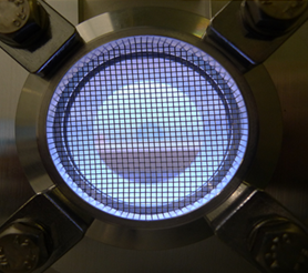
PLD Pulsed Laser Deposition

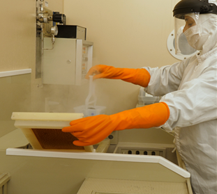
Standard depos. Standard chemical and physical deposition cleanroom/lab processes
UV-SL UV-Soft lithography
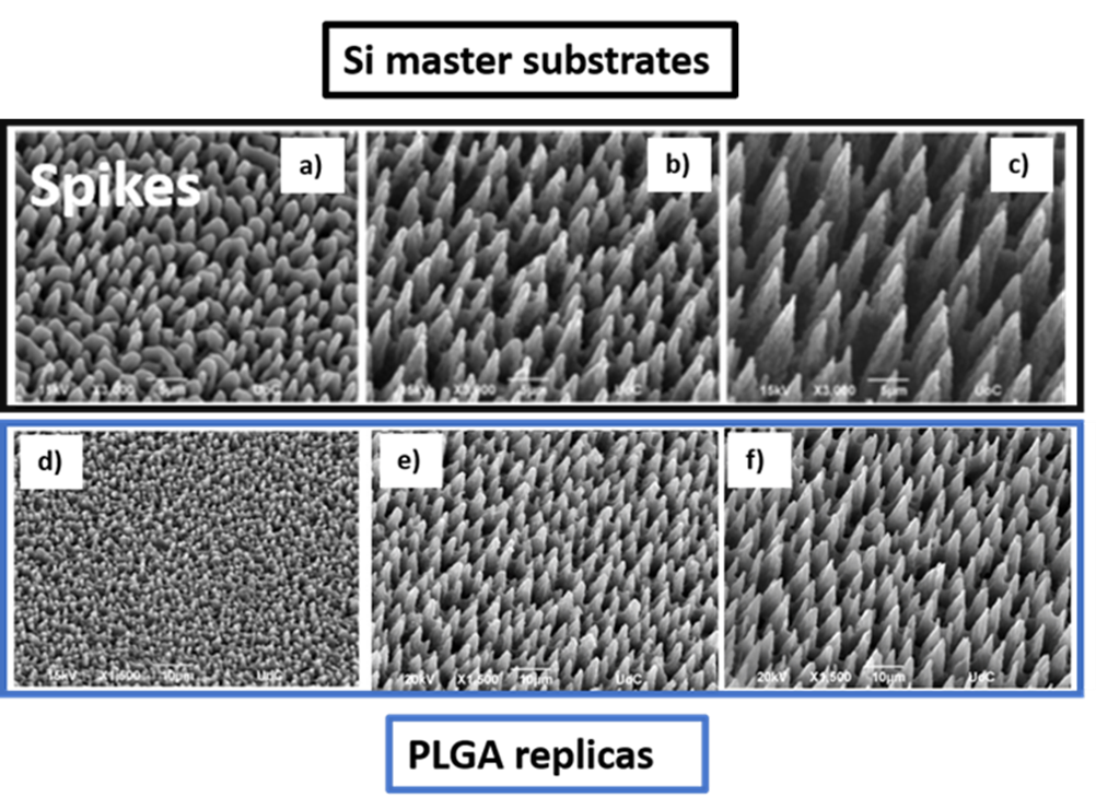
Standard etching Standard dry/wet patterning cleanroom/lab processes