Atomic Layer Etching
Lithography & Patterning (Patterning, replication, and sample navigation)
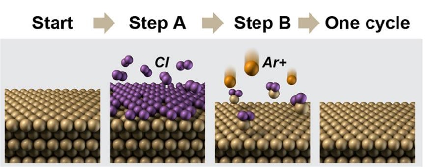
Atomic layer etching (ALE) is a nanofabrication technique, with high precision and control of material removal at the atomic level. The concept is analogous to atomic layer deposition (ALD), except that removal occurs in place of a second adsorption step, resulting in layer-by-layer material subtraction instead of addition. The key distinguishing feature of ALE compared to other dry etching techniques is its sequential, self-limiting nature, where each etching cycle removes precisely one atomic layer. This level of control is paramount for achieving nanoscale precision and maintaining uniformity across surfaces.
The ALE process typically takes place in two steps: a surface reaction and a volatile by-product removal step. First, the surface is dosed with an etchant flux and the etchant is pumped down. In this step, a specific chemical species reacts with the material to be etched, forming a chemisorbed layer. Then ion enhanced etching removes the monolayer of the material which has been dosed and the volatile product is pumped down. This self-limiting mechanism ensures that only one atomic layer is removed in each cycle, preventing over-etching, and maintaining precision. At the same time, most ALE reactors can also operate as inductively coupled plasma (ICP) etchers with gas flow pulsing and precise ion energy control.
One of the key aspects of ALE is its ability to etch a wide range of materials, including semiconductors, dielectrics, and metals, with atomic precision. This versatility makes it a valuable tool in the field of nanofabrication. Moreover, ALE allows for selective etching, enabling the removal of specific materials while preserving others - a crucial capability for creating intricate patterns and structures. Beyond semiconductors, ALE has applications in diverse fields like in the development of nanoelectromechanical systems, nanophotonics, sensors, optical components, energy storage devices, and bioelectronics.
Instruments datasheets
Also consider
MT Magneto-transport

ALD Atomic Layer Deposition


