CM is used to determine the surface contours and profiles of micro-structured components and to quantify the height and depth of features; it is also able to build a 3-D image with structure information below the surface.
CM offers several advantages over conventional optical microscopy, including shallow depth of field, elimination of out-of-focus glare, and the ability to collect serial optical sections from thick specimens.
In conventional microscopy, the sample is placed on the microscope stage and the entire field of the specimen is illuminated and visualized. Although the highest intensity is at the focal point of the objective lens, other parts of the sample are illuminated generating background “noise” which compromises the quality of the image. However, in confocal microscopy, the incoming light is focused through the microscope objective on a small spot inside the microstructure. The same objective gathers the reflected or fluorescent light coming back from the sample. A small pinhole aperture in a screen is used so that only the light emitting from the desired focal spot is can pass through. The screen blocks any light scattered outside the focal plane. In optical terms, the pinhole is placed in a conjugate focal plane of the sample (hence the designation “confocal”). A sensitive light detector, such as a photomultiplier tube, on the other side of the pinhole to detects the confocal light. Thus the specimen can be imaged one “point” at a time.
To create virtual-sectioned images of the microstructure, the focal spot is serially scanned in the X–Y plane. As the scanning progresses, signal from the detector is fed to a computer that collects all the “point images” of the sample and serially constructs the image one pixel at a time. Because the sample is not actually sectioned, it is possible to image and display a “stack” of virtual, confocal images a video monitor and achieve a high-contrast image that could not be acquired by conventional microscopy.
Optical profiler
Confocal microscopy and interferometry
Confocal: 10x-20x-50x-150x
Interferometer: 10x and 20x
Dual LED light
Confocal: max 1 nm vertical resolution for areas from 85 mm x 64 mm (150x) to 1270 mm x 950 mm (10x)
Interferometer: max 1 nm vertical resolution for areas of 640 mm x 480 mm
Stitching capability for larger area characterization
Confocal: up to 0.1 4mm3 (150x)
Interferometer: up to 0.31 mm3 (blue light)
In SEM a beam is scanned over a sample surface while a signal from secondary or back-scattered electrons is recorded. SEM is used to image an area of the sample with nanometric resolution, and also to measure its composition, crystallographic phase distribution and local texture.
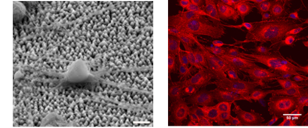
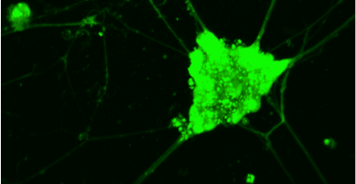
The Cell Culture Facility provides the necessary equipment (basic cell culture, sample preparation, functional assays and imaging equipment) for the study of the effect of biomaterials on specific cell behavior and function and cellular responses, such as cell survival, adhesion, morphology, proliferation, growth, migration and differentiation.
The “Live Cell Imaging” facility is equipped with advanced imaging microscopy techniques (based on two- or multi- photon excitation), which are appropriate for the all-optical minimally invasive, high-resolution (<500nm), deep (>500μm) monitoring of living cells and tissues for long periods of time.
In TEM/Scanning TEM (STEM) high energy electrons incident on ultra-thin samples, allow imaging, diffraction, electron energy loss spectroscopy and chemical analysis of solid materials with a spatial resolution on the order of 1-2 Å. Samples must have a thickness of a few tens of nanometres and are prepared in sample preparation laboratory.
Laser patterning is a technique for the controlled patterning of materials at micro- and nano-scales. It offers the ability to directly write patterns on the surface and complex 3D channels into the bulk of solid materials, also biomaterials. Applications can range from microfluidic systems and sensors to tissue engineering scaffolds.