Laser surface and in-volume Patterning

Nano to Micro/Macro (3D shaping)

Laser precision fabrication offers the ability for the surface and in-volume patterning, at the micro- and the nano- lengthscales, of practically all classes of solid materials, including biomaterials. The inhomogeneous energy absorption along with material resolidification and related self-assembly phenomena, are the key factors towards precise control of the morphological features for various applications, including tailoring of wettability, controlling fluid transport, tuning of adhesion and friction, tailoring optical properties, as well as improving the biocompatibility and bioactivity of tissue scaffolds. Apart from self-assembled, (pseudo)periodic and hierarchical structures formation, laser precision micro/nano fabrication can be employed for direct writing via material ablation, welding and sintering.


@
          provided at NFFA-Europe laboratories by:
CSIC-IO
Spain
FORTH
Greece
EURONANOLAB
France

Instruments datasheets

EURONANOLAB
France
LSIVP at EURONANOLAB - FEMTO-ST
The LSIVP is limited to transparent materials (normally glass, fused quartz and similar materials) - more materials MAY BE available.
EURONANOLAB
France
LSIVP at EURONANOLAB - MMI
na
na
yes
no
na
0
CSIC-IO
Spain
Pulsed Excimer Laser Annealing
Lambda Physik LPF200
Large area sample annealing (up to a few square cm via sample scanning)
no
no
tif
100
laser wavelength 193 nm, pulse duration 20 ns, spot size 0.5x0.5 cm^2 up to 1x1 cm^2
400 mJ/pulse
motorized sample scanning, 5x5 cm^2, 10 um resolution
air
in-situ CCD camera
CSIC-IO
Spain
Pulsed excimer laser interference patterning
Lambda Physik LPF200
Direct laser interference patterning with ns UV laser
no
no
tif
100
laser wavelength 193 nm, pulse duration 20 ns, spot size 0.5x0.5 cm^2
Fluence: 0.2 - 1.8 J/cm^2
yes
air environment
in -situ CCD camera
pattern type: parallel fringes with smallest period 1.4 um
CSIC-IO
Spain
Femtosecond laser surface structuring via beam scanning
Satsuma HP2
Femtosecond laser surface structuring of materials for functional applications
no
no
tif
100
laser wavelength: 1030 nm, 515 nm, pulse duration: 280 fs, repetition rate up to 2 MHz
beam scanning with F-theta lens
air
CSIC-IO
Spain
Femtosecond laser surface structuring via sample scanning
Satsuma HP2
Femtosecond laser surface structuring of materials for functional applications
no
no
tif
100
laser wavelength: 1030 nm, 515 nm, pulse duration: 280 fs, repetition rate up to 2 MHz
sample scanning with high precision x-y-z motors
air
in-situ microscope
CSIC-IO
Spain
Femtosecond direct laser interference patterning
Spectra Physics Tsunami & Spitfire Pro
Femtosecond laser surface structuring of materials for functional applications
no
no
tif
100
laser wavelength 800 nm, pulse duration 120 fs, max. 1 kHz
0.5 mJ
sample scanning
in-situ microscope
fabrication of periodic line and dot structures. minimum period 1.25 um
CSIC-IO
Spain
Femtosecond pump-probe microscopy during laser processing
custom-built
time-resolved microscopy studies with sub-ps temporal and micrometric spatial resolution upon fs pulse excitation
no
no
tif
1000
pump pusle: 800 nm, 120 fs, probe pulse: 400 nm, 100 fs
in-situ microscope
CCD camera, field of view 300 x 200 um
CSIC-IO
Spain
Real-time reflectivity measurements with ns resolution during laser processing
home-built
time-resolved reflectivity studies with ns temporal upon fs and ns pulse excitation
no
no
txt
10
pump: 800 nm, 120 fs or 8 ns, probe: 532 nm or 1064 nm, cw
in-situ microscope
fast photodiodes
@
          provided at NFFA-Europe laboratories by:
CSIC-IO
Spain
FORTH
Greece
EURONANOLAB
France

Also consider

Structural & Morphology Characterization

SEM Scanning Electron Microscopy

In SEM a beam is scanned over a sample surface while a signal from secondary or back-scattered electrons is recorded. SEM is used to image an area of the sample with nanometric resolution, and also to measure its composition, crystallographic phase distribution and local texture.

Theory & Simulation

MMMEI Multiscale modeling of materials under extreme irradiation

This techniques offers a multi-scale theoretical framework that allows for the estimation of structural and phase changes when materials are exposed to extreme irradiation conditions generated by various types of electromagnetic sources (e.g. synchrotron sources, pulsed and free-electron lasers).

Electronic & Chemical & Magnetic Characterization

OS Optical spectroscopy

VUV/UV/Vis/NIR spectroscopy is the measurement of the attenuation of a beam of light after it passes through a sample or after reflection from a sample surface. It is useful to characterize absorption, transmission, and reflectivity of a variety of technologically important materials, such as gases, film, pigments, coatings, windows, and filters.

Nano to Micro/Macro

LCI Live cell imaging

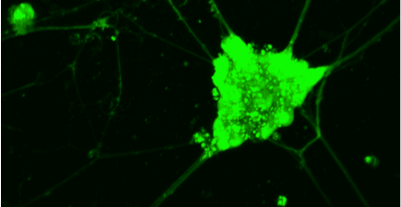
The “Live Cell Imaging” facility is equipped with advanced imaging microscopy techniques (based on two- or multi- photon excitation), which are appropriate for the all-optical minimally invasive, high-resolution (<500nm), deep (>500μm) monitoring of living cells and tissues for long periods of time.

Structural & Morphology Characterization

AFM Atomic Force Microscopy

AFM is a surface sensitive technique permitting to obtain a microscopic image of the topography of a material surface and certain properties (like friction force, magnetization properties…). Typical lateral image sizes are within a range of only a few Nanometers to several Micrometers, and height changes of less than a Nanometer.