While the origins of ultraviolet photoelectron spectroscopy (UPS) were in the spectroscopy of free molecules in the gas phase, in the context of micro/nano structures or nanomaterials, it is typically applied to measurements on solid surfaces, where it is also known as photoemission spectroscopy (PES).
In laboratory variants of UPS instruments, a helium gas discharge lamp is typically used as the photon source, with access to either HeI (21.2 eV) or HeII (40.4 eV) photons. The low energies of the incident photons and ejected photoelectrons are the basis for surface sensitivity of UPS measurements, with the majority of the measured photoelectrons originating within the topmost few nm of the sample. The much lower energy of the photon source compared to those used in the x-ray photoelectron spectroscopy (XPS), limits UPS to measurements of valence-band features close to the Fermi level, but such features can be measured with higher precision and resolution by UPS than by XPS. A particularly useful application of UPS is the determination of the work function of a material.
The USP measurements must be carried out in an ultra-high vacuum (UHV) chamber. Accordingly, the auxiliary features available in a laboratory UPS system, such as sample heating or cooling, vary depending on the setup of that UHV chamber. Often, a He-lamp source is attached as an auxiliary source to an XPS system, making features such as sputtering sources (based on monoatomic, molecular, or cluster ions) available for sample cleaning or depth profiling before or during UPS measurements.
Ultraviolet photoelectron spectroscopy (UPS), also described as photoemission spectroscopy (PES) when applied to measurements on solid surfaces, is a technique suitable for measuring the spectral features that are close to the Fermi level for surfaces or adsorbates. UPS is particularly useful for determining the work function and the electronic properties of valence band of a material.
Only for standard measurements. Will be decided by the instrument scientists.
no
EURONANOLAB
France
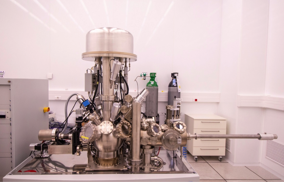
UPS at EURONANOLAB - PoliFAB
AU-ISA
Denmark
UPS - MatLine beamline @ASTRID2
MatLine is dedicated to the electronic properties of surfaces and interfaces on metal, metal oxide and semiconductor, especially of adsorbed molecules on substrates.
Multi-pole wiggler from ASTRID2; Resolving power 200 to 3,500; Typical Flux 1x10¹¹ photons/sec; Spot size: 0.7 mm X 0.7 mm.
SPECS PHOIBOS 150 1D-DLD electron analyzer
Temperatures in the range of 110K – 1200K; Non-insulating samples at size less than 12mm X 7mm X 2mm; Possibility of measuring certain type of powders
Measurements are carried out under UHV
2 evaporator ports (CF40), installation without break main vacuum; gas inlet; load-lock; auto heating while measuring; LEED; ion gun; RESPED is not available at the moment
no
na
20-700 eV, with the possibility up to 1260eV at lower resolution and flux
XPS is a surface spectroscopic technique for quantitative measurements of the elemental composition or stoichiometry and the chemical state of the present elements, like their oxidation state and chemical bonds. XPS is highly surface sensitive, giving chemical and binding energy information from the a narrow region close to the surface.
In TEM/Scanning TEM (STEM) high energy electrons incident on ultra-thin samples, allow imaging, diffraction, electron energy loss spectroscopy and chemical analysis of solid materials with a spatial resolution on the order of 1-2 Å. Samples must have a thickness of a few tens of nanometres and are prepared in sample preparation laboratory.
Soft X-rays XAS operating at Ambient Pressure allows for in-operando spectroscopic investigation of surfaces and their catalytical properties. This opens interesting access to L and M-edges of most of the transition metals and K-edges of light elements (C, O and N). The high surface sensitivity is achieved by the total electron yield detection.
This technique offers the possibility of simulating structural and electronic properties based on the electronic ground state, including electronic charge analysis, energetics of formation, structural and vibrational properties; IR, Raman, EPR, NMR, core-level XAS & XPS, STM & AFM.
XAS is sensitive to the local bonding environment of the atom absorbing the X-rays, providing information on oxidation states, local orbital symmetry, molecular orientation and chemically selective density of states. It is widely used in molecular and condensed matter physics, material science, engineering, chemistry, earth science and biology.