Electron and ion beam lithography
He-FIB He-Focused Ion Beam & He-microscopy
With He-FIB, it is possible to achieve sub 10-nm feature sizes, not possible with traditional FIB. He and Ne ion beams are used to fabricate ultrahigh-resolution structures with speed and ease by lithography (using a resist), by direct milling or by ion-beam induced deposition (with special gas precursors).
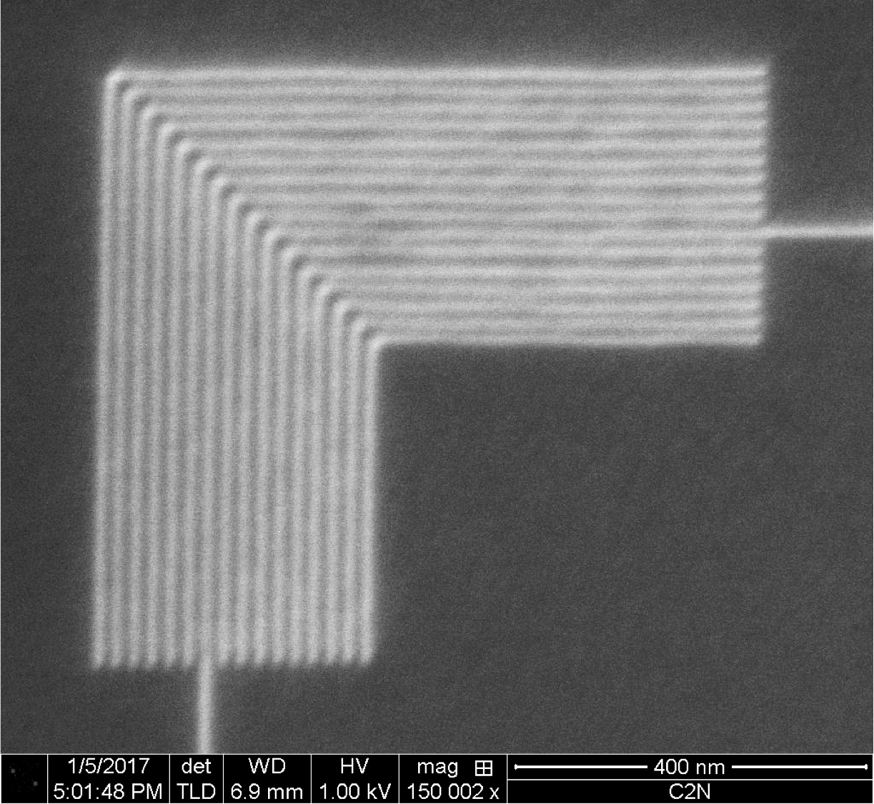
EBL Electron Beam Lithography

Electron-beam lithography is a direct write nanopatterning technique utilizing a finely focused electron beam in order to write nanoscale patterns on special e-beam resists in two and three dimensions. Compared to other nanostructuring methods, it stands out for its high level of flexibility and resolution and reasonable patterning speed.
FIB Focused Ion Beam

By FIB, usually combined with an electron column, it is possible to achieve 2D and 3D nanometric structures, either by ion milling or by ion/electron beam disposition, with a high degree of control and flexibility. Electrical measurements and other characterization are possible. It is a good technique to prepare samples for TEM investigations.

