Displacement Talbot Lithography (DTL)
Lithography & Patterning (Photon-based lithography)
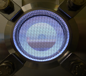
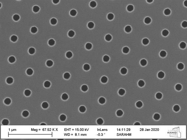
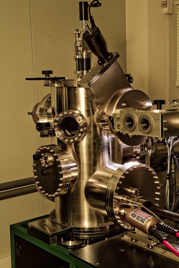
Displacement Talbot lithography is a novel optical interference technique based on the Talbot effect, suitable for mass-fabrication of high-resolution periodic structures. It can reproducibly achieve subwavelength resolutions on a wafer scale. Moreover, since it is a parallel patterning method, it is extremely fast. A phase shift mask containing a periodic pattern is illuminated with UV or DUV light, such that the region below the mask contains a 3D diffracted light field. The mask pattern is replicated by intense light peaks on vertically spaced planes through this region. During the exposure, the samples undergo several cycles of vertical displacement through multiple copies of the pattern. This unique 3D exposure method renders patterns with high depth-of-focus, making it insensitive to wafer bowing or uneven sample surfaces. The features are produced in a consistent way across the entire wafer allowing patterning also in thick photoresists. Since no mechanical contact is made between the sample and mask this method is well suited to delicate materials. Depending on the application, the technique can be combined with lift-off, dry etching, electroplating or any other pattern transfer technique. Submicron feature sizes, such as linear gratings and two-dimensional hexagonal or square arrays of holes can be achieved at a wafer scale. By tuning the accumulated dose for the exposure, different feature dimensions can be obtained.
Also consider
EBE e-beam evaporation
Standard etching Standard dry/wet patterning cleanroom/lab processes
SEM Scanning Electron Microscopy

AFM Atomic Force Microscopy

Standard depos. Standard chemical and physical deposition cleanroom/lab processes