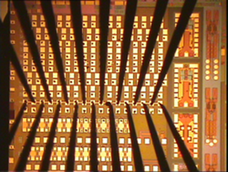
Microprobe electrical testing
Nano to Micro/Macro (Electrical analysis)
The step of local electrical characterization of layers or devices usually occurs at the end of the manufacturing process, when the fabricated wafers must be tested before being cut and used singularly. In assessing the material quality and device reliability, it is important to have non-destructive, accurate and easy-to-use electrical characterization techniques available, so that important parameters (sheet resistance, contact resistance, semiconductor bulk defect density, type and mobility of carriers, interface quality, oxide defects density, oxide dielectric behaviour...) can be rapidly determined.
Probe stations are been designed to allow access to the test pads of the fabricated circuits and test structures at chip and wafer level (before the encapsulation step and having the wafers diced), and so allowing the full measurement range of today’s most advanced test instrumentation, such as impedance analysers, semiconductor parameter analysers, picoamperimeters, electrometers, voltage and current sources, etc. and without the parasitics introduced by the wiring to the chip package. When measuring in single chips several independent probes can be flexibly used allowing at leat 2-probe or 4-probe characterizatons. The same arrangement can be used when measuring at wafer level, but also fixed collective probe cards adapted to the pads lay-out are preferable.
The available set of instrumentation, along with a dedicated and properly designed set of test structures can fulfil the necessities of electrical characterization for a good number of applications, from device characterization, parametric test or IC failure analysis, to assessment of material quality, modelling, process development or design debug.
Instruments datasheets
Also consider
SEM Scanning Electron Microscopy

LSIVP Laser surface and in-volume Patterning

SMP Soft matter preparation


