Due to the upcoming SLS 2.0 and ELETTRA 2.0 upgrade, this technique will be unavailable at PSI and CNR-IOM(TS) until further notice.
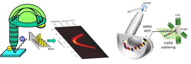
Angle Resolved Photoemission (ARPES) allows to measure directly the electronic band structure of crystalline solids. It is based on the photoelectric effect: the electron inside the solid absorbs energy and (negligible) momentum from the incoming photon and is ejected in vacuum where it is detected retrieving information about its initial state energy, momentum and spin. State of the art electron energy and momentum analyzers, and high energy resolution and polarization control of the exciting light are needed for resolving the fine electronic structure. Adding efficient spin-polarization measurement to ARPES, i.e. measuring Spin Polarized-ARPES at uncompromised energy and momentum resolution will enable addressing the study of the magnetic properties of surfaces, interfaces and nanostructures, as well as the spin-orbit coupling effects that determine the spin texture of the surface bands in complex materials of interest for their potential in spintronics.
Elettra synchrotron, Apple II Quasi-Periodic undulator; variable polarization (horizontal, vertical, circular ±); flux on sample @ 10µm slits (ph./s) >2 x 10¹¹; beam size on the sample 150x50 (HxV, µm2)
8-120 eV
VG Scienta DA30 analyzer; spin detection based on very low energy electron diffraction (VLEED) from magnetic surface oxide targets
(E/dE) 30000
T range: 15-300 K
Preparation chamber with 3 heating stages: HT (RT- 2000K), WT (170K - 900K), LT (RT - 700K); ion gun; 3 evaporator ports (CF40); gas inlet leak valve; LEED+AES (Omicron SPECTALEED)
Soft-x-ray-VUV and resonant angle-resolved photoelectron spectroscopy, resonant photoelectron diffraction, resonant x-ray photoemission spectroscopy, fast photoemission with selectable polarization;
core levels, valence band, work function, Auger, surface and bulk band dispersion, empty states in the conduction band, magnetic remanence, strain in thin films, time-resolved spectral evolutions during surface reactions
Elettra synchrotron, Apple II undulators; variable polarization (horizontal, vertical, circular ±); beam size on the sample 350x350 (HxV, µm2); vertical size can be reduced on request; flux on sample @ 10µm slits (best resolution) (ph./s) 2 x 10¹² -6 x 10¹⁰
35-1650 eV
VG Scienta R3000 analyzer with slit(s) perpendicular to the scattering plane
(E/dE) 20000-5000
Many samples can be accomodated in a 25x25 mm2 area; T range: 50-1200 K (PID-controlled)
Both preparation and main chambers with heating stages (e-beam, direct current, PBN), ion gun (VG), 4 evaporator ports (CF40), gas inlet valve (variable leak valve), diamond file scraper, cleaver; evaporators for organic molecules; e-beam evaporators (Omicron) for metals (evaporation at low sample temperatures is also possible); LEED (OciLEED)
XAS is possible in the same chamber; quick XPS acquisition mode (300 ms per spectrum); 4 degree-of-freedom manipulator (rotation axis perpendicular to the scattering plane); possibility to measure at T>300 K; electrical Insulation of the sample: possibility to apply a voltage and measure the work function; possibility to superimpose synchrotron beam to external light sources to study photoinduced phenomena
Base pressure: UHV
ICN2
Spain
ARPES
Band mapping, Fermi Surface
SPECS UVS 300 UV light with monochromator for He I (21.2 eV) and He II (40.8eV)
0-18eV or 0-38eV
SPECS PHOIBIOS-150 analyser
Angular resolution of 0.5 deg and total energy resolution down to 3meV
T down to 80K, heating to 700K
Preparation chamber equipped with heating stage (e beam), sputter gun, load lock, LEED, gas inlet leak valve and 3 evaporation ports
Soft-X-ray radiation, Resonant Inelastic X-ray Scattering (RIXS) and ARPES
Fixed-gap undulator, circular and 0-180o variable linear polarization, flux on sample up to 1013 ph/s/0.01%BW/400 mA, spot size 10x74 µm2 (ARPES); 4x52 µm2 (RIXS)
300 - 1600 eV
PHOIBIOS-150 analyser, constant angular dispersion through the whole operative energy range
Better than 0.07o at 1 keV; up to 33000 (E/ΔE, 1 keV)
Temperatures down to 10.5 K
Transfer chamber equipped with LEED, load-lock, low-T cleavage, preparation chamber: gas exposure, ion bombardment, heating up to 1000oC, and thin film deposition
The Surface and Interface Spectroscopy (SIS) beamline provides a state-of-the-art experimental set-up to study the electronic band structure of novel complex materials by spin- and angle-resolved photoelectron spectroscopies. The beamline has been designed for the energy range from 10 to 800 eV with high flux, high resolution, variable polarization, and low high-harmonic contamination
EM crossed field undulator, linear horizontal (10 - 800 eV), linear vertical (100 - 800 eV), circular left/right (50-800 eV) , flux at 200 eV 2x10¹³ ph/s/0.1%BW/0.4A, spot size on sample at 200 eV 50μm x 100μm
10 - 800 eV
VG-SCIENTA R4000 photoelectron spectrometer for a total angular acceptance of 30 degrees
Up to 10000 (E/ΔE)
Temperatures down to 10 K and up to 400 K, sample dimensions: diameter < 10mm, thickness ~0.1 - 3mm
In-situ cleaving, sample preparation and characterization chamber: ion sputtering, annealing (300K-1000K), LEED
Spin- and angle- resolved photoemission spectroscopy endstation available
UHV
CARVING manipulator
PSI
Switzerland
ARPES, XPD - PEARL Beamline @ Swiss Light Source Synchrotron
The PEARL (Photoemission and atomic resolution laboratory) beamline is dedicated to the structural characterisation of local bonding geometry of molecular adsorbates on metal or semiconductor surfaces, of nanostructured surfaces, and of surfaces of complex materials. It is a soft X-ray beamline with an angle-resolved photoelectron spectrometer for angle-scanned and photon energy-scanned X-ray photoelectron diffraction (XPD)
Bending magnet, linear horizontal, partial circular left/right, flux on sample at 1 keV: 2x10¹¹ph/s, spot size: 170μm H x 73μm V, FWHM, 1mm x1mm
Max sample size 8x8 mm, thickness 2 mm, mounted on flag style sample plates (Mo or Cu).
Cryogenic manipulator 5 degrees of freedom (x,y,z, polar angle and tilt), down to 20 K
Sample heating stage up to 1000 degrees by electronic bombardment
Ar ion sputtering
In vacuum cleaver
Sample garage
time resolved ARPES, XPS
SEM, TEM
Chemical laboratory
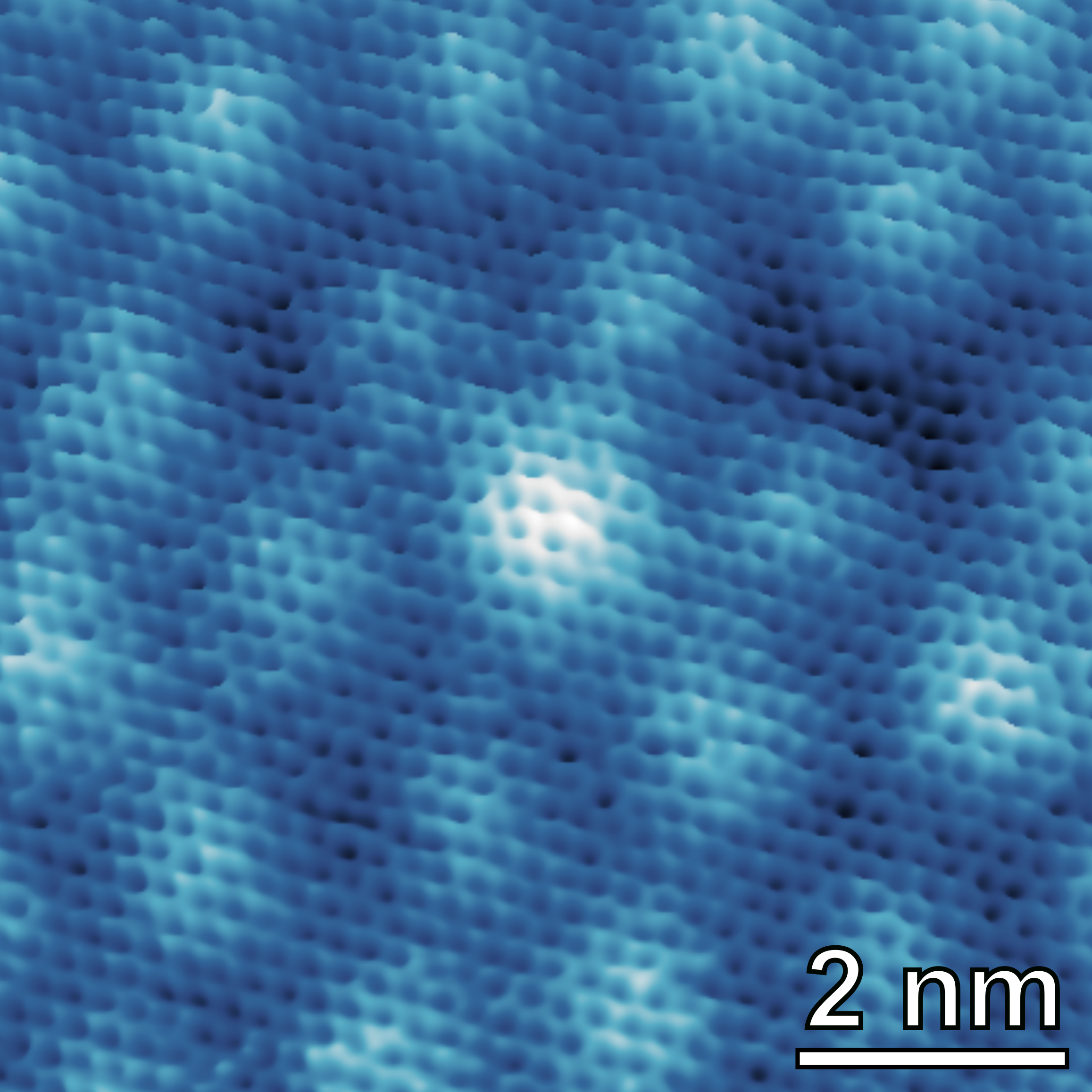
STM allows imaging conductive surfaces at the atomic scale. It is possible to characterize the distribution of surface terraces and steps, as well as to determine the atomic arrangement of (ordered) surface (over)structures.
XRD provides non-destructive information on the structural order of a material. At large scattering angles XRD permits to identify different crystal phases and to quantify lattice distances and crystalline volume fractions. At low angles of incidence the surface roughness of a single crystal and the thickness of a deposition layer can be obtained.
XPS is a surface spectroscopic technique for quantitative measurements of the elemental composition or stoichiometry and the chemical state of the present elements, like their oxidation state and chemical bonds. XPS is highly surface sensitive, giving chemical and binding energy information from the a narrow region close to the surface.
This technique offers the possibility of simulating structural and electronic properties based on the electronic ground state, including electronic charge analysis, energetics of formation, structural and vibrational properties; IR, Raman, EPR, NMR, core-level XAS & XPS, STM & AFM.
PLD is widely used to grow thin films of complex oxides and other inorganic and organic materials. It is a simple and versatile technique based in the congruent ablation of a solid material irradiated by an ultraviolet laser.