The cathodoluminescence tool is a SEM with a FEG source (2-10 keV) allowing spatial resolution as low as 3 nm. Luminescence spatial resolution from 10 nm to several hundreds of nanometers depending on electron beam energy and probed material. It can be used for analysis of material properties (charge carrier recombination, electronic transition) and detection of defects or impurities. Helium to room temperature luminescence characterization of solid samples using steady-state excitation (simultaneous mapping of cathodoluminescence, EBIC and SEM) and pulsed excitation (time-resolved cathodoluminescence). Time-resolved (available only at C2N-CNRS) is detected either with a Hamamatsu streak camera, or with a Time-Correlated Single Photon Counting (TCSPC) module equipped with a PM or an APD detector. Temporal resolution down to 10 ps.
The samples are mounted on a 1 inch sample holder attached on a piezoelectric nano-positioning cryostage allowing low temperature measurements (~10K). An intra-column optical collection system coupled with a dispersive spectrometer and two array detectors permits the spectral analysis of luminescence emission from 200 nm to 1.6 µm. This system offers a way to extract spatially resolved electronic and/or optical properties of luminescent material and devices.
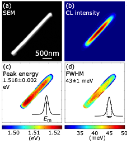
Helium to room temperature luminescence characterization of solid samples
Analysis of material properties (charge carrier recombination, electronic transition) and detection of defects or impurities
Electron gun with a beam current varying from 100pA to 20nA, focused on the sample thanks to a SEM microscope
Luminescence spatial resolution from 30nm to several hundreds of nanometers depending on electron beam energy and probed material
SEM resolution is few nanometers
Secondary vacuum ambient in the chamber
Helium cryostat from 4 K to 500 K
Cross section view is possible, in this case sample size is limited to 2mmx2mm
Sample preparation allowed: cleaving or polishing only
No FIB etching (detrimental for luminescence characteristics of a lot of materials)
In TEM/Scanning TEM (STEM) high energy electrons incident on ultra-thin samples, allow imaging, diffraction, electron energy loss spectroscopy and chemical analysis of solid materials with a spatial resolution on the order of 1-2 Å. Samples must have a thickness of a few tens of nanometres and are prepared in sample preparation laboratory.
XPS is a surface spectroscopic technique for quantitative measurements of the elemental composition or stoichiometry and the chemical state of the present elements, like their oxidation state and chemical bonds. XPS is highly surface sensitive, giving chemical and binding energy information from the a narrow region close to the surface.
PL is a non-contact, non-destructive method of probing the electronic structure of materials, often used in the context of semiconductor devices to determine the bandgap energy, the composition of heterostructures, the impurity levels, the crystal quality, and to investigate recombination mechanisms.
This technique offers the possibility of simulating structural and electronic properties based on the electronic ground state, including electronic charge analysis, energetics of formation, structural and vibrational properties; IR, Raman, EPR, NMR, core-level XAS & XPS, STM & AFM.
The pump-probe spectroscopy infrastructure provides in-situ probes of the excited state of the matter, i.e. in the time/frequency domain at the fs-ps scales.