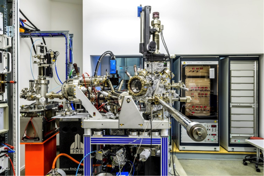
SPELEEM microscope is being used by a broad range of researchers from different scientific areas such as materials science, nano-science and technology, physics, chemistry, and biophysics. Here are the main imaging modes of the SPELEEM microscope:
- X-ray Photoemission Electron Microscopy (XPEEM). Energy filtered imaging (elemental/chemical mapping). - X-ray Magnetic Circular (Linear) Dichroism (XMCD, XMLD). Imaging of magnetic domains in ferromagnets (XMCD) and in antiferromagnets (XMLD) on the nm scale. - Micro-X-ray Photoemission Spectroscopy (micro-XPS). Photoelectron spectroscopy from extremely small areas down to a fraction of a micron.
- Micro-X-ray Absorption Spectroscopy (XAS). Imaging of secondary electron emission at fixed kinetic energy as a function of the photon energy.
- PhotoElectronDiffraction( PED). The intensity of a core level line as a function of energy and emission angle is measured. The technique can provide spatially resolved information on the surface crystallographic structure and is therefore complementary to LEED and STM. If the valence band electrons form a diffraction pattern, the band- and Fermi surface mapping in the full cone becomes possible (micro-ARPES). - Low Energy Electron Microscopy (LEEM). Study of morphology of crystalline surfaces. Several contrast mechanisms (including Dark Field Imaging) allow the determination of the lateral dimensions of regions with a given crystal structure, the thickness distribution of thin overlayers with monolayer resolution, the imaging of monoatomic surface steps and other morphological features) - Micro-Low Energy Electron Diffraction (micro-LEED). The diffraction patterns can be collected from areas as small as 100nm.
In TEM/Scanning TEM (STEM) high energy electrons incident on ultra-thin samples, allow imaging, diffraction, electron energy loss spectroscopy and chemical analysis of solid materials with a spatial resolution on the order of 1-2 Å. Samples must have a thickness of a few tens of nanometres and are prepared in sample preparation laboratory.
XRD provides non-destructive information on the structural order of a material. At large scattering angles XRD permits to identify different crystal phases and to quantify lattice distances and crystalline volume fractions. At low angles of incidence the surface roughness of a single crystal and the thickness of a deposition layer can be obtained.
XPS is a surface spectroscopic technique for quantitative measurements of the elemental composition or stoichiometry and the chemical state of the present elements, like their oxidation state and chemical bonds. XPS is highly surface sensitive, giving chemical and binding energy information from the a narrow region close to the surface.
This technique offers the possibility of simulating structural and electronic properties based on the electronic ground state, including electronic charge analysis, energetics of formation, structural and vibrational properties; IR, Raman, EPR, NMR, core-level XAS & XPS, STM & AFM.
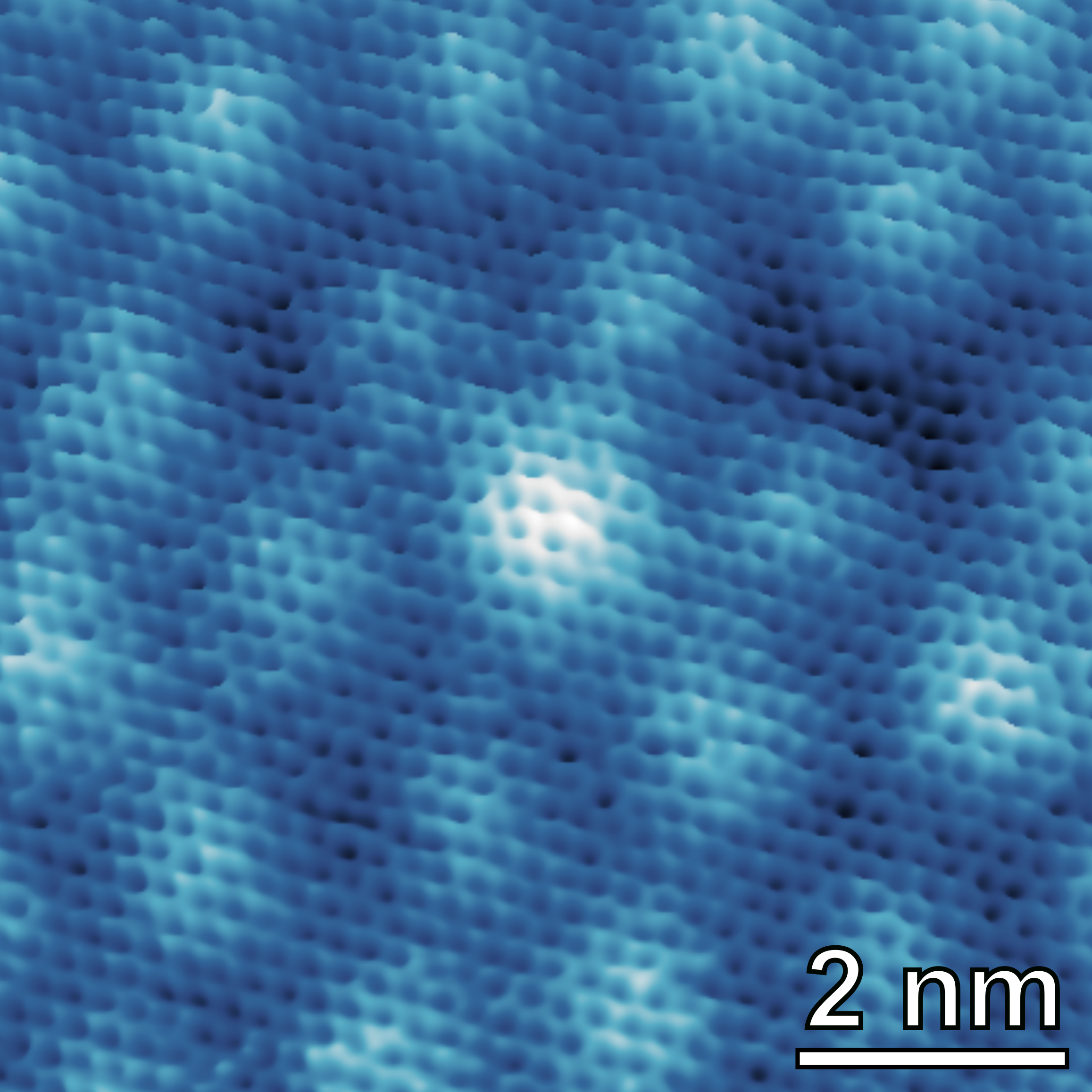
STM allows imaging conductive surfaces at the atomic scale. It is possible to characterize the distribution of surface terraces and steps, as well as to determine the atomic arrangement of (ordered) surface (over)structures.