This technique is encased in the direct laser writing family. Many UV photosensitive materials can similarly polymerize by the simultaneous absorption of two near IR photons (TPP: two photon polymerization). The chance of occurrence of this non-linear optical process is increased when an ultrashort pulse laser is focused tightly in a small given area. The size of this area depends on the laser spot and power, and on the properties of the material itself. Features in the vicinity of 100 nm are possible. By precisely scanning the laser focus throughout the material (or by moving the resist relatively to the fixed laser spot) a 3D extended volume can be affected, within the spatial limitations of the moving stage. As in any photolithographic process the chemical difference between unexposed and exposed volumes leads to selective material removal inside a developer bath. 3D arbitrary patterns can be defined in this way. As a particular case the laser can be constrained to a 2D pattern.
Examples of these materials are IPx photoresists, AZ resists family or SU-8. The photopolymers used can be commercially available, but also custom-developed materials by FORTH (such as ultra-high-resolution organic-inorganic hybrids, metal-binding materials, fluorescent and nonlinear materials.)
In many cases, polymers can be already the structural material required. If other materials, such as metals, silica, etc. are needed, the 3D patterns can be transferred from polymeric templates using inversion and casting techniques.
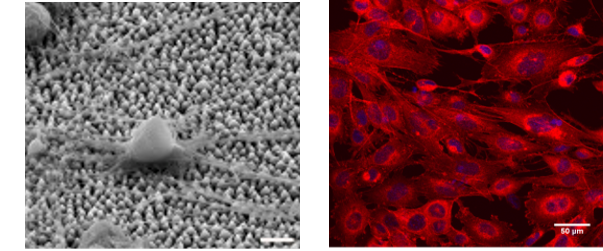
In SEM a beam is scanned over a sample surface while a signal from secondary or back-scattered electrons is recorded. SEM is used to image an area of the sample with nanometric resolution, and also to measure its composition, crystallographic phase distribution and local texture.
Laser patterning is a technique for the controlled patterning of materials at micro- and nano-scales. It offers the ability to directly write patterns on the surface and complex 3D channels into the bulk of solid materials, also biomaterials. Applications can range from microfluidic systems and sensors to tissue engineering scaffolds.
The Cell Culture Facility provides the necessary equipment (basic cell culture, sample preparation, functional assays and imaging equipment) for the study of the effect of biomaterials on specific cell behavior and function and cellular responses, such as cell survival, adhesion, morphology, proliferation, growth, migration and differentiation.
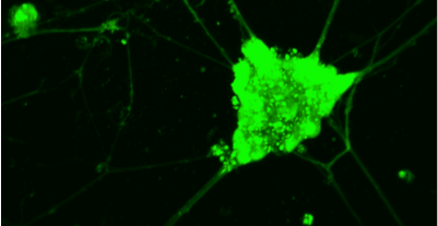
The “Live Cell Imaging” facility is equipped with advanced imaging microscopy techniques (based on two- or multi- photon excitation), which are appropriate for the all-optical minimally invasive, high-resolution (<500nm), deep (>500μm) monitoring of living cells and tissues for long periods of time.
Different nanochemical methodologies are offered to prepare nanomaterials (nanoparticles, nanowires, nanodots, self-assembled monolayers, films, nanoparticles, liposomes, emulsions, vesicles, etc). Among the systems that can be prepared are organic, hybrid organic-organic organic-inorganic, polymeric and biomaterial systems.