Spray-assisted layer by layer
Nano to Micro/Macro (thick films and coatings production)
Novel synthesis procedures and exploitation of nanostructure concept and assembling of polymers and/or nanoparticles (including also hybrids with several nanoparticles) in complex hierarchical structures have contributed to tremendous diffusion of multifunctional and smart coatings in several applications fields including packaging, cultural heritage, energy and environment, health care and transport. These coatings are currently designed to exhibit simultaneously several competitive properties (ie barrier, antimicrobial, antiscratch, conductive, antistatic, hydrophobic/hydrophilic, sensing and electromagnetic shielding, …). Furthermore they can also be designed to be “smart” coatings, able to adapt to external stimuli (ie anticorrosion coatings with stimuli-responsive release of anticorrosion, self-healing coatings,…) and reversible (ie prompt to be reshaped in the framework of sustainable and circular economy)
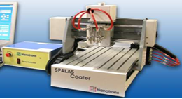
The Spray-assisted layer by layer has four replaced spray nozzle (to deposit two-three different coatings, in a LbL structure), may be programmed to spray on substrates up to 15x20cm2, allows deposition of cationic/anionic polymer solutions as well as nanoparticles dispersions (such as clay, halloysite and graphene and its derivatives) able to assemble with the polymeric phases with intermediary washing and drying and coat also complex surface as tubes and fibers
Instruments datasheets
Also consider
SAXS Small Angle X-ray Scattering

PA Permeability analysis
SEM Scanning Electron Microscopy

TEM Transmission Electron Microscopy


