When linearly polarized light is reflected from a magnetic film, its polarization becomes elliptic (Kerr ellipticity) and the polarization principal axis is rotated (Kerr rotation). This rotation is proportional to a component (depending on the geometry of experiment) of the magnetization of the film. For this reason the MOKE magnetometry is a very popular tool for the characterization of the magnetic properties of materials.
Since the laser spot can be focused down to a few microns, the magnetic properties (e.g. coercivity, squareness ratio) of single micrometer or submicrometer structures can be evaluated. With a suitable set-up the sensitivity of the MOKE apparatus can be pushed to detect the signal coming from very thin films (ideally down to the atomic plane) making the technique suitable for the study of magnetic structure of thin films, interfaces and nanostructures.
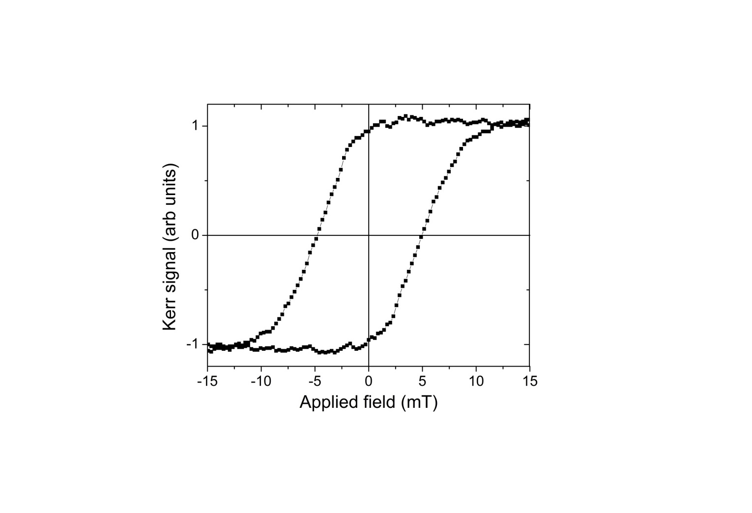
Note that although this technique can be very sensitive, no quantitative measure of the magnetization is provided. Nevertheless, from the shape of the hysteresis loop, both static and dynamic magnetization reversal processes can be investigated in detail. Longitudinal and polar configurations are used routinely to detect the in-plane or the out-of-plane magnetization components, respectively. This technique is well suited to characterize either flat or micron- and submicron-patterned films.
XRD provides non-destructive information on the structural order of a material. At large scattering angles XRD permits to identify different crystal phases and to quantify lattice distances and crystalline volume fractions. At low angles of incidence the surface roughness of a single crystal and the thickness of a deposition layer can be obtained.
PLD is widely used to grow thin films of complex oxides and other inorganic and organic materials. It is a simple and versatile technique based in the congruent ablation of a solid material irradiated by an ultraviolet laser.
XPS is a surface spectroscopic technique for quantitative measurements of the elemental composition or stoichiometry and the chemical state of the present elements, like their oxidation state and chemical bonds. XPS is highly surface sensitive, giving chemical and binding energy information from the a narrow region close to the surface.
In TEM/Scanning TEM (STEM) high energy electrons incident on ultra-thin samples, allow imaging, diffraction, electron energy loss spectroscopy and chemical analysis of solid materials with a spatial resolution on the order of 1-2 Å. Samples must have a thickness of a few tens of nanometres and are prepared in sample preparation laboratory.
In FIB an energetic beam of ions creates local removal of material by sputter erosion. Combination with an electron column, allows 2D and 3D nanometric structures to be achieved. Characterization by different detectors (SEM, BSE, STEM, X-Ray) is possible. FIB is the preferred technique to prepare extremely thin slices for TEM investigations.