Time Resolved Luminescence Spectroscopy
Electronic & Chemical & Magnetic Characterization (Luminescence spectroscopy)
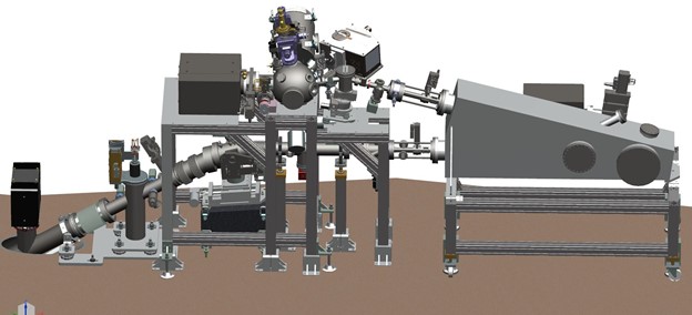
P66 serves as a specialized materials science beamline at the PETRA III synchrotron ring. Designed for precision photoluminescence experiments, the beamline offers temporal and spectral resolution, enabling detailed investigations of solids under state-selective excitation through pulsed synchrotron radiation. Central to the beamline's functionality is a double-grating, 2-meter McPherson primary monochromator operating at normal incidence (15⁰) (as depicted in the right portion of Figure 1). This primary monochromator facilitates sample excitation within the 3.7-40 eV energy range.
Samples under investigation are securely mounted on a cryostat double-sided holder (90x30 mm), positioned within a spherical sample chamber shown in the upper section of Figure 1. Throughout the experiments, the samples are maintained in ultrahigh vacuum conditions. Typically, the beamline is employed to analyze various solid-phase materials, including single crystals, glasses, ceramics, films, and powders. The experimental setup allows for the recording of time-resolved emission, excitation, and steady-state reflection and absorption spectra. Emission spectra can be recorded in 110-1200nm range.
The unique pulsed nature of synchrotron radiation enables the accumulation of luminescence decay kinetics spanning from 160 ps to 192 ns. Time-resolved measurements are conducted utilizing the time-correlated photon counting method. The start marker for these measurements is synchronized with the PETRA III bunch clock. Photon registration is performed using a Hamamatsu MCP R3809U-50 detector, and events are recorded by a Cronologic xTDC4 time-to-digital converter card. The full width at half maximum (FWHM) of the system's response function is approximately 160 ps, aligning with the duration of the synchrotron pulse.
Also consider
SEM Scanning Electron Microscopy

XPS X-ray Photoelectron Spectroscopy

XRD X-Ray Diffraction

OS Optical spectroscopy

FIB Focused Ion Beam


