Physical depositions of thin films
PVDS PVD sputtering
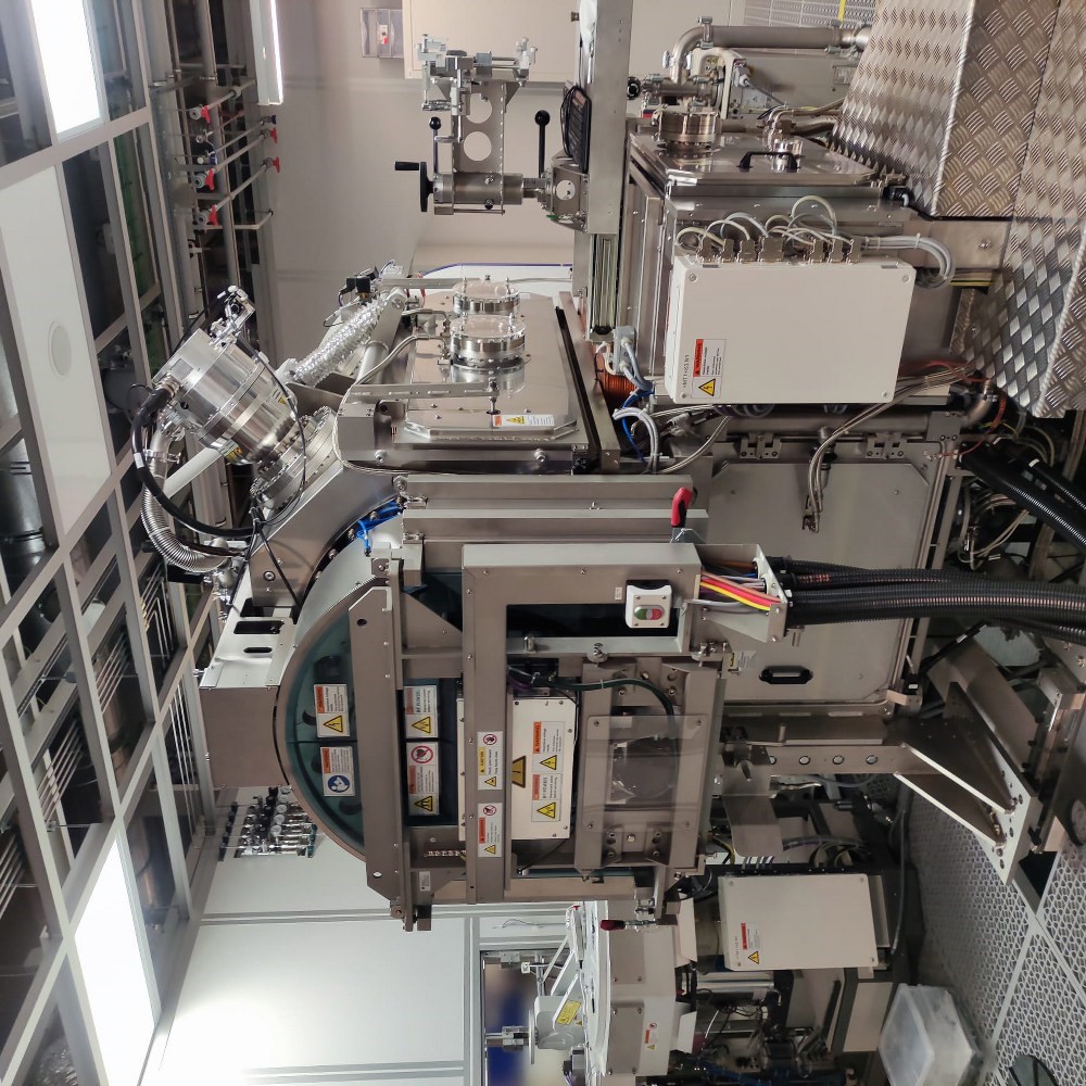
Physical vapor deposition (PVD) by sputtering is a process whereby a material is sputtered from a solid target and deposited on a substrate as a film or coating, with thicknesses from sub-nm to several microns, in mono-layered, multi-layered, or multi-graduated structures and well-controlled morphology.
PLD Pulsed Laser Deposition
PLD is widely used to grow thin films of complex oxides and other inorganic and organic materials. It is a simple and versatile technique based in the congruent ablation of a solid material irradiated by an ultraviolet laser.
EBE e-beam evaporation
E-Beam evaporation is a physical vapor deposition (PVD) technique whereby an intense electron beam is generated from a filament and steered via electric and magnetic fields to strike the source material (e.g. pellets of Au) and vaporize it within a vacuum environment.
TE Thermal evaporation
Thermal evaporation is a simple high-vacuum physical vapor deposition method for depositing thin films of materials (few Å to few hundred nm). The technique involves the joule-heating of a solid source material that evaporates and deposits on the substrate. Common deposited materials are Al, Ag, Ni, Cr, Au, In, among many others.
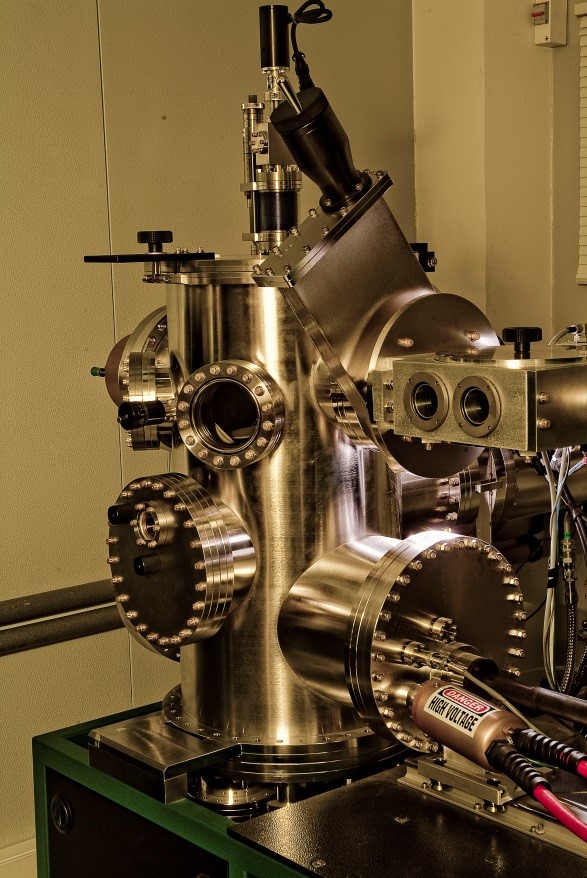
MBE Molecular Beam Epitaxy
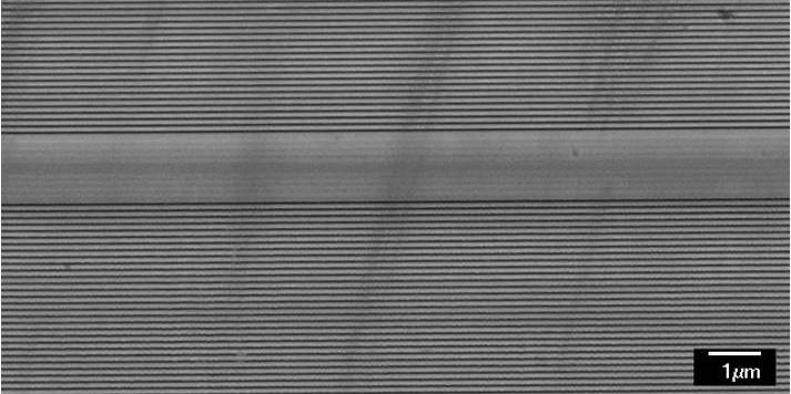
MBE allows growth of high quality semiconductors, oxides and organic epitaxial layers, with crystal structure commensurate with the substrate. It is used to build nanostructures (quantum dots, nanowires), layered heterostructures for lasers, photodetectors, LED and optoelectronic devices.
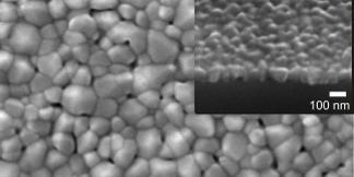
MS Magnetron sputtering
This is a simple physical method to deposit, in form of thin film or multilayers, a wide variety of materials from simple metals to complex inorganic structures, between few Angstroms and hundreds of nanometers. The technique is based on the evaporation of solid surface by field-accelerated ions of a heavy gas that are focused by a magnetic field.

