PVD sputtering
Growth & Synthesis (Physical depositions of thin films)
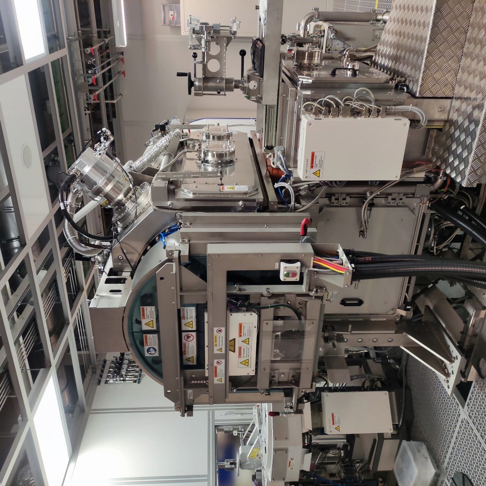
Physical vapor deposition (PVD) by sputtering has been developed as a complementary approach to the traditional PVD using evaporation sources. The control of the properties and transfer of the target material using sputtering enables deposition of films for applications that impose stringent requirements on the high morphological quality and composition of surfaces, e.g., roughness, grain size, or stoichiometry. To deposit such high-quality films, PVD Sputtering systems are typically optimized for relatively low deposition rates, which enable reproducible deposition of films down to sub-nm thickness.
Both DC and RF magnetrons are commonly used as power sources for sputtering in PVD. With an appropriate design of the sputtering sources, both conductive and insulating materials can be deposited using this approach.
Commercial PVD Sputtering tools are often equipped with clusters of sources, to enable deposition of stacks of different materials without breaking the vacuum, which helps to ensure the high quality of the interfaces between the layers. Common applications that benefit from the high quality of stacks deposited by PVD Sputtering include multilayers for advanced magnetic or tunneling devices. Additional capabilities in PVD Sputtering systems can include substrate heating, application of a magnetic field, mechanical movement to produce wedge layers, or automated systems for handling wafers. The wide use of the PVD Sputtering tools in the industry also makes this approach beneficial for projects that aim at the eventual technology transfer to industrial partners.