Lithography & Patterning
Scanning probe lithography View all
DPN Dip-pen Nanolithography (DPN)
Scanning probe lithography (SPL) methods have unique strengths in terms of resolution, throughput and patterning speed. Generally, SPL methods utilize the excellent control over positioning and movement of a tip or sample stage for highly localized additive and maskless deposition of chemical compounds or carrier fluids with functional components.
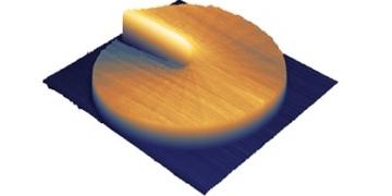
AFML Atomic Force Microscopy Lithography
In AFM, short range tip-sample interactions provide insight into phenomena taking place at the surface: catalysis, friction, low dimensional magnetism... The knowledge can be used to modify the surface to create nanometer scale patterns providing a true 3D reconstruction of patterns during the fabrication process.
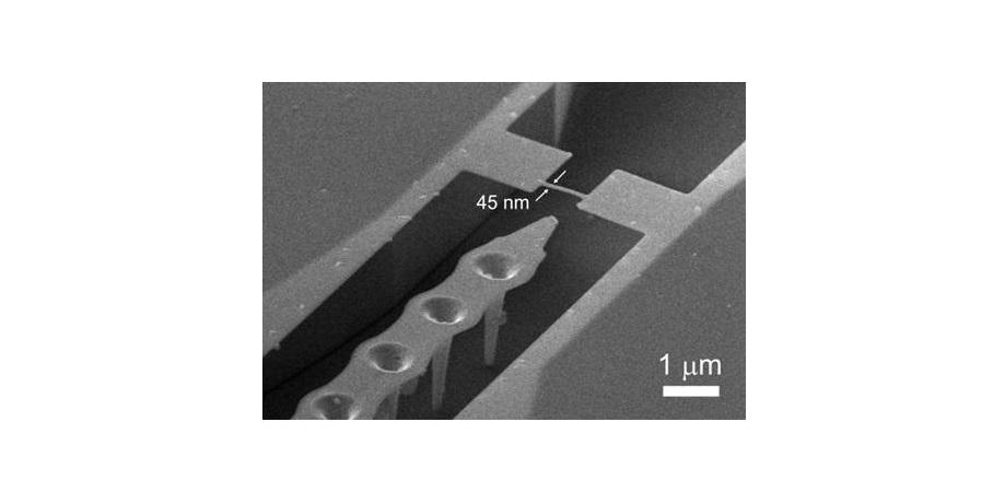
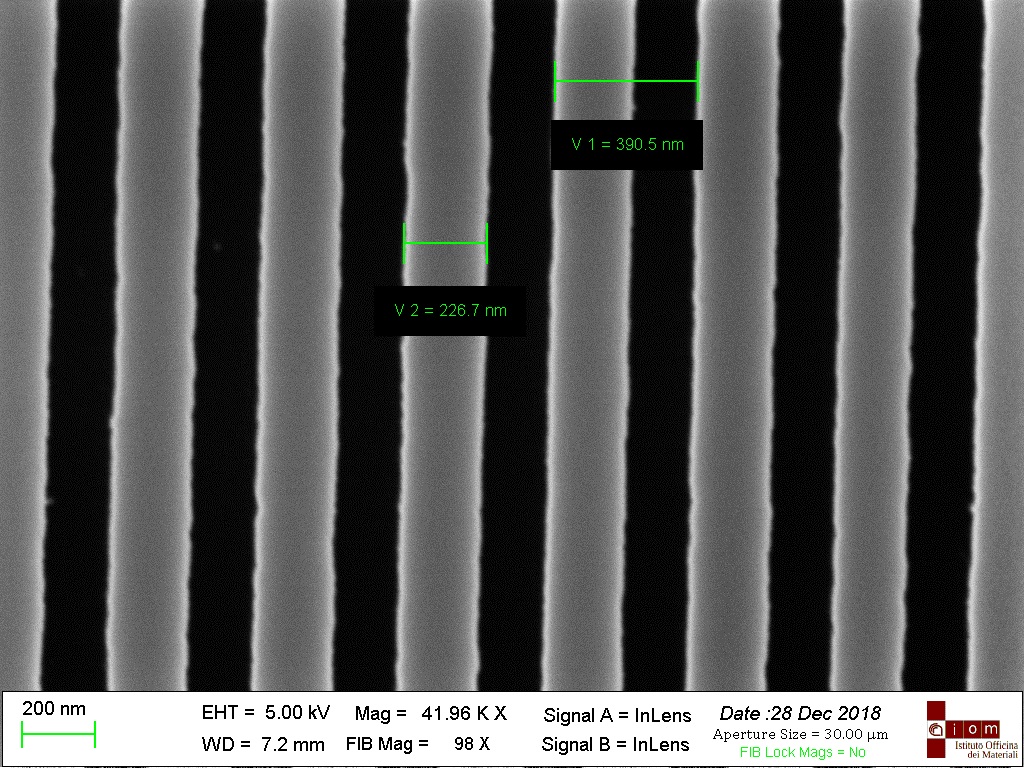
T-SPL Thermal Scanning Probe Lithography
T-SPL is a mask-less, serial and direct-write lithography technique, where a cantilever with a heatable ultra-sharp silicon tip (few nanometers in diameter) is brought into contact with a special resist that is spin-coated on a substrate. It can be used to create sub-10 nm structures as well as complex, high resolution 3D shapes.
Patterning, replication, and sample navigation View all
ICP Inductively Coupled Plasma
ICP is a reactive ion etching technique, where plasma is generated by means of inductively coupling RF power in the source. The ion energy bombarding the substrate is independently controlled via the applied bias power. This allows for a wide process space to address from anisotropic deep etching to highly chemical or physical processes.
RIE Reactive Ion Etching
RIE is used to etch various materials under vacuum in the presence of reactive ions. The sample to be etched is placed in a vacuum chamber and gas is injected into the process chamber via a gas inlet in the top electrode. The lower electrode is negatively biased and a single RF plasma source determines both the ion density and their energy.
IBM Ion-beam milling
Ion beam milling is a pattern transfer technique used to etch thin films of materials by physical sputtering or milling by use of a broad ion beam. The beam energy, the beam-to-substrate angle as well as the sample rotation speed can be selected for tunable etching conditions according to the application.
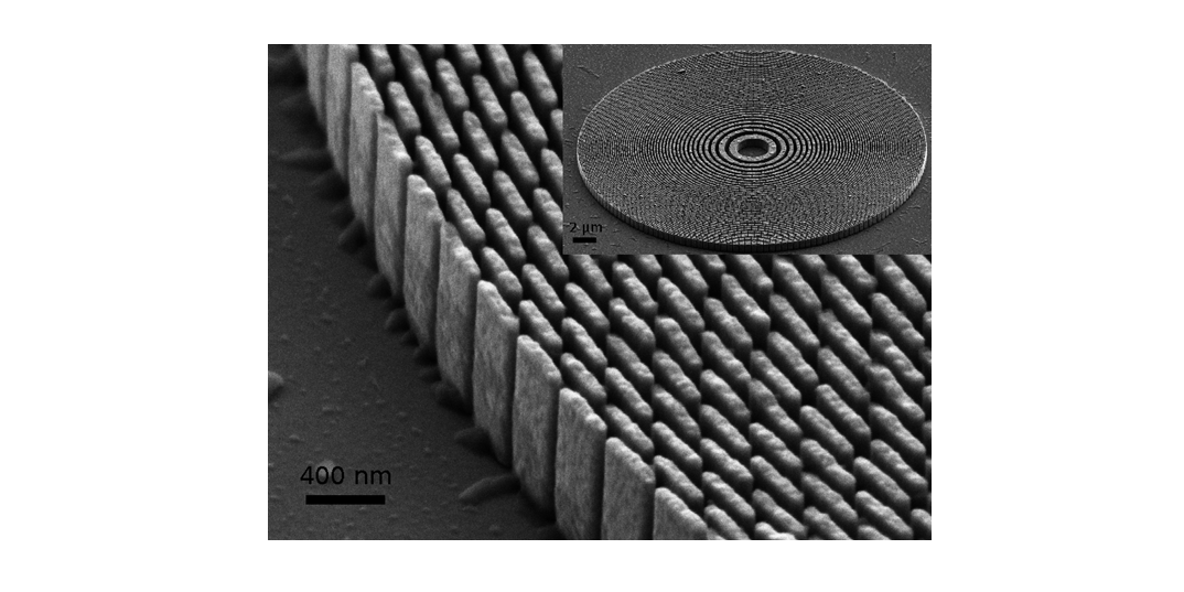
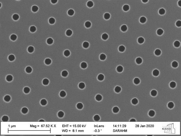
NIL NanoImprint Lithography
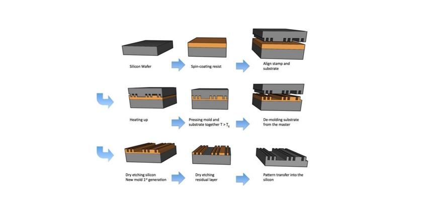
NIL is a low cost, high resolution and high-throughput method for nanoscale patterning. It creates patterns by mechanical deformation of an imprint resist and subsequent processes. NIL is one of the most promising next generation techniques for large area replication in the nanometer scale. Thermal and UV assisted NIL is possible.
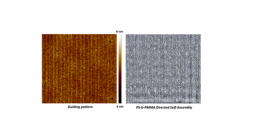
BCL Block copolymer lithography
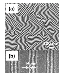
BCP lithography takes advantage of the self-assembly properties of BCPs to create nanoscale surface patterns in large areas. The main advantages is the process simplicity, the spatial resolution and the high throughput. Block co-polymer patterns are transferred to the substrate by etching using one of the BCP phases as an etching mask.
NOT&P Nano-Object Transfer & Positioning
Nano-Object Transfer & Positioning permits identifying, marking, and transferring pre-selected nano- and microscale single objects and enables their multi-analytical characterization by re-localization with different nano-science instruments at labs and ALFSs.
ALE Atomic Layer Etching
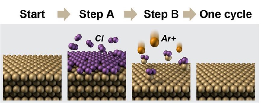
Atomic layer etching is a plasma etching process occurring in cycles of gas dosing and ion bombardment that removes material layer by layer. It has the potential to remove single atomic layers with very low damage. It uses a classical ICP reactor with the additional ability to dose etchant gases and accurately control the ion bombardment energy.
Electron and ion beam lithography View all
He-FIB He-Focused Ion Beam & He-microscopy
With He-FIB, it is possible to achieve sub 10-nm feature sizes, not possible with traditional FIB. He and Ne ion beams are used to fabricate ultrahigh-resolution structures with speed and ease by lithography (using a resist), by direct milling or by ion-beam induced deposition (with special gas precursors).
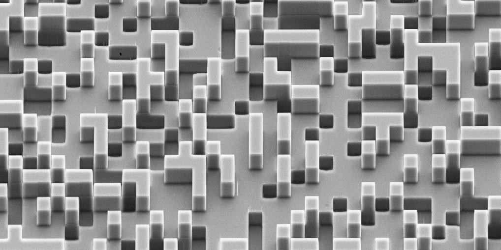
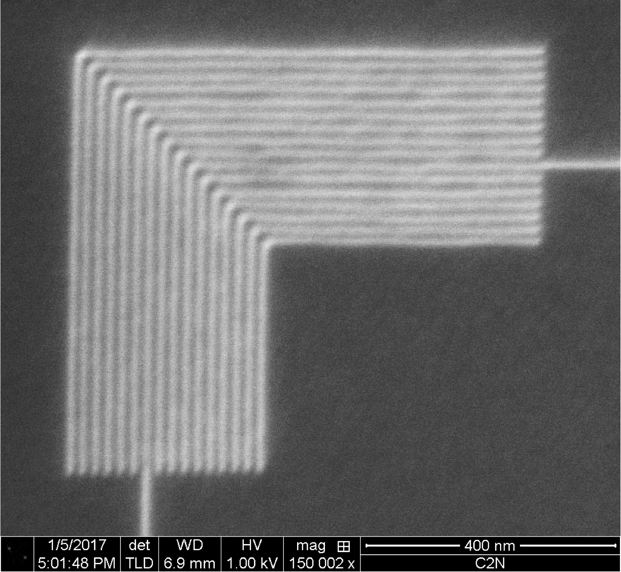
EBL Electron Beam Lithography
Electron-beam lithography is a direct write nanopatterning technique utilizing a finely focused electron beam in order to write nanoscale patterns on special e-beam resists in two and three dimensions. Compared to other nanostructuring methods, it stands out for its high level of flexibility and resolution and reasonable patterning speed.
FIB Focused Ion Beam
By FIB, usually combined with an electron column, it is possible to achieve 2D and 3D nanometric structures, either by ion milling or by ion/electron beam disposition, with a high degree of control and flexibility. Electrical measurements and other characterization are possible. It is a good technique to prepare samples for TEM investigations.
Synchrotron-based lithography View all
EUV-IL Extreme Ultra Violet - Interference lithography (temporarily unavailable)
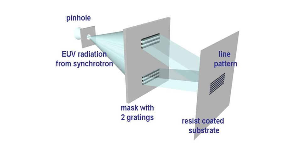
EUV interference lithography is a powerful tool both for scientific and industrial research. A spatially filtered beam from the synchrotron is projected on a mask through multiple gratings. The diffracted beams interfere on a wafer coated with a photosensitive polymer. Periodic patterns down to single digit resolution can be achieved.
DXRL Deep X-Ray Lithography
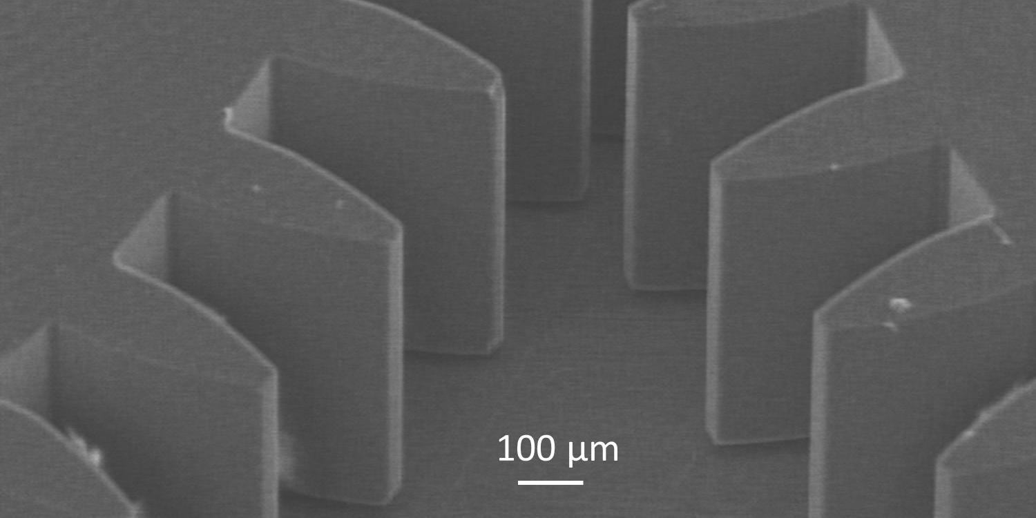
DXRL allows controlled irradiation of samples with high energy X-rays (2–20 keV). It offers high penetration depth, min lateral resolution of 200 nm, high aspect ratio, vertical sidewalls, optical surface quality. It is used to produce plastic microdevices, or of other materials following the LIGA process (lithography, electrodeposition, moulding).
Photon-based lithography View all
SM-DWL Submicron Direct Write Lithography (Binary/Grayscale)
Direct write lithography is a maskless patterning method to produce arbitrary features over large areas. A focused light source is scanned over a surface and exposes a resist according to a CAD design. This technique can be thought as a replacement for a mask aligner with the added capability of spatially modulating the dose (grayscale patterns).
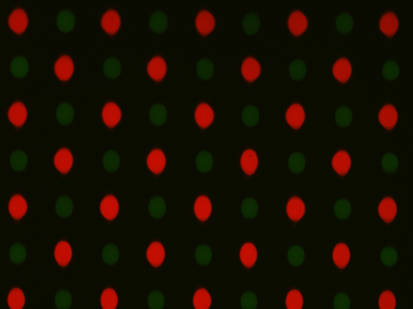
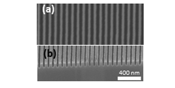
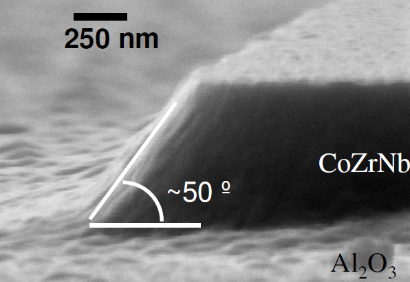
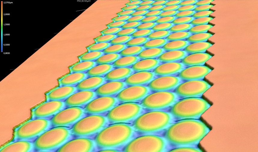
UV-IL Ultra Violet - Interference lithography
Laser interference lithography is designed for the fabrication of high quality submicrometer size gratings and arrays over an area of a few cm2. The modulation of the array features is obtained by fine tuning the exposure incidence angle. In this configuration low defect density and high reproducibility are enabled.
DTL Displacement Talbot Lithography (DTL)
Displacement Talbot Lithography is a contactless method to produce regular features over large areas. A 3D diffraction pattern is formed below a mask with a periodic pattern. A photoresist-coated substrate is moved vertically through this pattern so the effective dose is integrated in space and time forming a collapsed version of the pattern.
TWL Two-photon Lithography

HR 2D and 3D structuring process of a photosensitive material by physical and chemical changes produced in the focusing area of an ultrashort pulse laser of sufficiently high light intensity. 2D resist mask-less patterns, or polymeric micro-parts with a 3D shape can be obtained by scanning the photoresist relative to the beam focus submicron.

