He-Focused Ion Beam & He-microscopy
Lithography & Patterning (Electron and ion beam lithography)
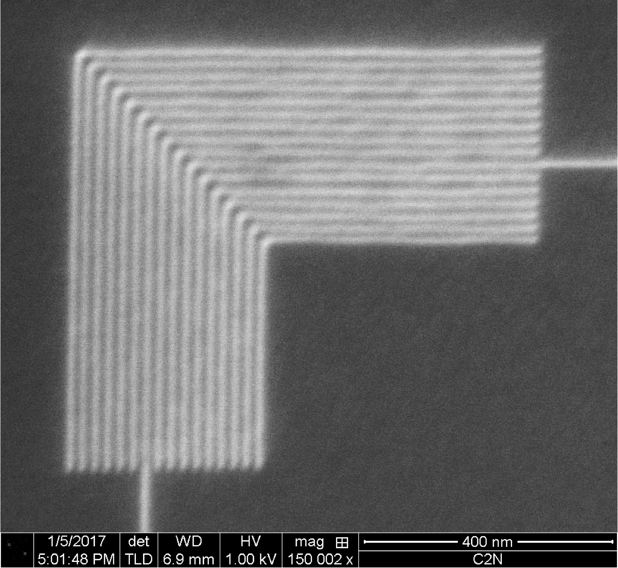
Individual atoms are stripped away from a finely sharpened needle until an atomic pyramid is created with just three atoms at the very end of the source tip – a configuration called the trimer. Once the trimer is formed, the tip is maintained under high vacuum and cryogenic temperatures with helium or neon gas flowing over it. By applying a high voltage to the needle, the He or Ne atoms are ionized in the vicinity of a single atom. This produces an extremely bright beam that can be focused with an advanced electrostatic column to an extraordinarily small probe size. He and Ne atoms have a smaller De Broglie wavelength and a smaller area of surface interaction than electrons and can, therefore, achieve higher resolution. With the use of an electron flood gun charge compensation can be achieved for use with insulating materials. Patterning can be performed by direct milling (material removal) with the He or Ne atoms or by exposing a resist without any proximity effects as is usually the case with electron beam lithography. The technique can also be used for additive nanopatterning, where high-quality conductive and insulating materials can be deposited with ion-beam induced deposition. Since He or Ne is used, undesirable Ga-implantation does not occur leading to high material purity and minimized changes to the properties of the materials. In addition, the tool can be used for high-resolution imaging (0.5 nm) with very large depth of focus.
Also consider
SEM Scanning Electron Microscopy

XPS X-ray Photoelectron Spectroscopy

AFM Atomic Force Microscopy

EBL Electron Beam Lithography


