Submicron Direct Write Lithography (Binary/Grayscale)
Lithography & Patterning (Photon-based lithography)
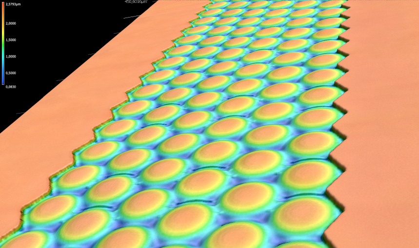
Direct writers are more and more replacing optical mask aligners that were for a long time the workhorses in cleanroom-based patterning of large, wafer-like substrates. This is possible because they offer reasonable resolution in the micrometer and often submicrometer scale, while offering high throughput. Since conventional UV lithography requires a mask that has to be prepared in advance, direct writing has evolved as a more flexible and versatile method. The design from a CAD program can be directly converted into the format suitable for direct write lithography and the resist (positive or negative) can be directly patterned. Standard processes are available for a range of materials. Even dose variations can be included, making DWL a fast and reliable process. Overlay of different layers is possible, too, enabling the manufacturing of complex devices, on chips from a few square mm up to 200 mm wafers and even more. DWL machines for resist patterning are considered as complement between high resolution electron beam writers and additive 3D methods using 2-photon processes or inkjet-based tools. But they offer more: They are capable to pattern 3D structures by varying the exposure dose, while scanning over the resist. Then grayscale (2.5 dimensional) structures can be patterned over large surfaces with submicron features in thin resist or high aspect ratio structures in films up to 50 to 100 µm. For this, proximity effects and resist nonlinearities must be considered. The technique has applications in microoptics, microfluidics, microelectronics etc.