Ultra Violet Spectroscopy
Electronic & Chemical & Magnetic Characterization (Electron spectroscopy)
While the origins of ultraviolet photoelectron spectroscopy (UPS) were in the spectroscopy of free molecules in the gas phase, in the context of micro/nano structures or nanomaterials, it is typically applied to measurements on solid surfaces, where it is also known as photoemission spectroscopy (PES).
In laboratory variants of UPS instruments, a helium gas discharge lamp is typically used as the photon source, with access to either HeI (21.2 eV) or HeII (40.4 eV) photons. The low energies of the incident photons and ejected photoelectrons are the basis for surface sensitivity of UPS measurements, with the majority of the measured photoelectrons originating within the topmost few nm of the sample. The much lower energy of the photon source compared to those used in the x-ray photoelectron spectroscopy (XPS), limits UPS to measurements of valence-band features close to the Fermi level, but such features can be measured with higher precision and resolution by UPS than by XPS. A particularly useful application of UPS is the determination of the work function of a material.
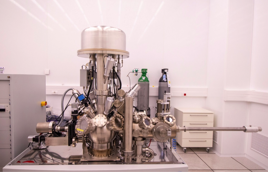
The USP measurements must be carried out in an ultra-high vacuum (UHV) chamber. Accordingly, the auxiliary features available in a laboratory UPS system, such as sample heating or cooling, vary depending on the setup of that UHV chamber. Often, a He-lamp source is attached as an auxiliary source to an XPS system, making features such as sputtering sources (based on monoatomic, molecular, or cluster ions) available for sample cleaning or depth profiling before or during UPS measurements.
Ultraviolet photoelectron spectroscopy (UPS), also described as photoemission spectroscopy (PES) when applied to measurements on solid surfaces, is a technique suitable for measuring the spectral features that are close to the Fermi level for surfaces or adsorbates. UPS is particularly useful for determining the work function and the electronic properties of valence band of a material.