Scanning tunneling microscopy (STM) allows imaging conductive surfaces at the atomic scale. It is possible to characterize the distribution of surface terraces and steps, as well as to determine the atomic arrangement of (ordered) surface (over)structures.
In STM, an atomically sharp tip is scanned on a surface at a few-angstrom distance, while a bias voltage is applied between these two electrodes, so that a current flows due to the quantum tunneling effect. The intensity of the tunneling current depends exponentially on the tip-surface distance and can therefore be used to reconstruct a morphologic image.
STM is a local technique: while high-resolution can be achieved on small (nanometer sized) areas, information on large-scale (micron sized or more) is lost, and measurements have to be repeated systematically on several regions of the sample to get statistically relevant information.
Due to stability performances, STM experiments are typically time-consuming. The technique is applicable both in air and in vacuum. Ultra-high-vacuum (UHV) is required for the characterization of delicate, atomically clean systems.
The STM signal is not purely topographic, but brings also information on the local density of electronic states. Scanning tunneling spectroscopy (STS) is an extension of STM that provides information about the density of electrons in a sample as a function of their energy. Inelastic tunneling spectroscopy (IETS) is a challenging extension for the investigation of vibrational states at liquid helium temperature. The STM tip can also be used to manipulate single atoms and molecules.
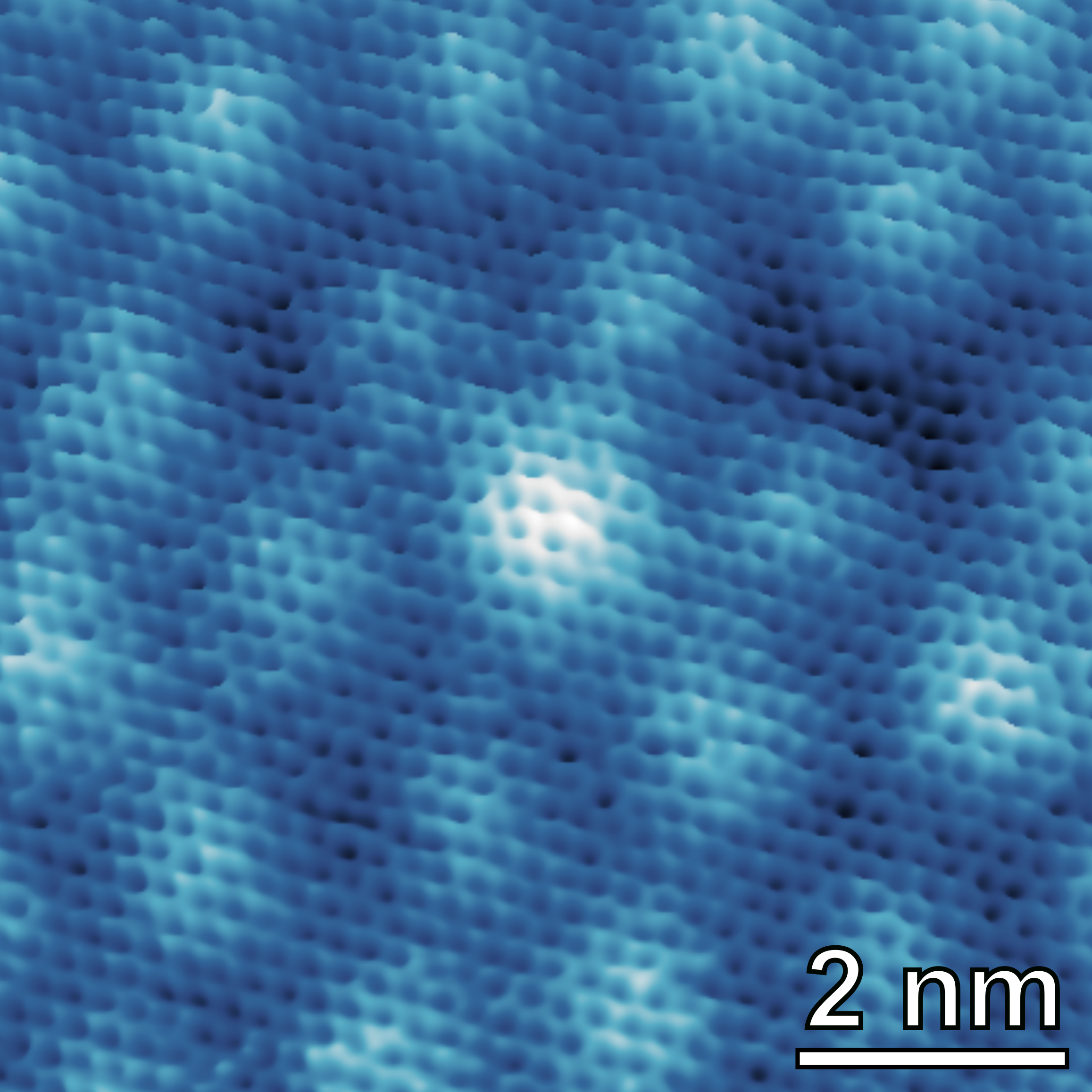
By acquiring sequences of consecutive images, STM can also be used to investigate at the atomic scale dynamical processes occurring on the surface of conductive samples, with a typical acquisition time of few tens of seconds per image. To further extend the range of accessible details in this kind of measurements, NFFA-Europe makes for the first time available to external users the access to a FastSTM option for high-speed imaging with a VT-STM microscope at CNR-IOM. Thanks to this option, it is now possible to image with atomic resolution dynamical processes as chemical reactions, diffusion and growth, with a frame rate up to 100 images per second on regions few-nanometer wide.
Characterisation of structural and electronic modifications at the atomic scale
Time resolution: ≥ 30 s/image
Sample size: ø ≤ 8mm
Sample preparation T range: 30K-1400K
UHV
Gas inlet: ≤10-5 mbar
T range: 2.5K-300K
LEED, QMS, knudsen cells, TPD
Electronic and vibrational local spectroscopy
Single atom/molecule manipulation
no
na
0
CNR-IOM @TS
Italy
VT-STM
na
Characterisation of structural and electronic modifications at the atomic scale
Time resolution: ≥ 30 s/image
Sample size: ≤ 9 x 7 mm2 x 1 mm or ø ≤ 7 mm x 1 mm
Sample preparation T range: 100K-1300K
UHV
Gas inlet: ≤ 10-6 mbar
T range: 300K-850K
LEED, QMS, evaporators, high pressure cell for sample preparation under gas exposure up to 10 mbar
System optimised for high-resolution and in-operando experiments.
FastSTM option available for imaging up to 100 images/s.
At the beta-test level, it is also possible to perform measurements in near ambient pressure of H₂, CO₂, and CO.
no
na
0
no
CNR-IOM @TS
Italy
FastSTM
na
Imaging of chemical reactions, growth processes, diffusion and reconstructions at the atomic scale
Time resolution: up to 100 images/s on 5 nm x 5 nm sample regions
Sample size: ≤ 9 x 7 mm2 x 1 mm or ø ≤ 7 mm x 1 mm
Sample preparation T range: 100K-1300K
UHV
Gas inlet: ≤ 10-6 mbar
T range: 300K-850K
LEED, QMS, evaporators, high pressure cell for sample preparation under gas exposure up to 10 mbar
Instrument offered as option for the VT-STM
System optimised for high-resolution and in-operando experiments
no
na
0
DESY + PETRA III
Germany
Temperature UHV STM/AFM @ DESY NanoLab
Topographic imaging of surfaces
Sub-atomic resolution in x, y, z by piezo scanner
Sample size: 10 mm x 10 mm
Variable temperature range: 50 K < T < 500 K (liquid N2 and option for He cooling)
10-10- 10-11 mbar base pressure
Access for optical microscope
Direct sample transfer under UHV from and to the UHV system
Omicron UHV STM/AFM instrument
High resolution quartz tuning fork AFM
STM tunnelling spectroscopy
AFM contact and tapping mode
Magnetic Force Microscopy (MFM) option
x-y translation: 10 mm x 10 mm
PSI
Switzerland
Surface Science Lab @ Laboratory for Micro- and Nanotechnology
STM
0.01Å
Anything conducting or semiconducting (pA)
UHV
W-Tip
pA
4x motors, 0.5μm x 0.5μm
1pA-1μA, -10V to +10V
CNR-IOM @TS
Italy
OSMOS: VT-STM + XPS + UPS
- On-surface synthesis and modification of organic molecules.
- Morphological, structural and chemical modification of self-assembled monolayers on surfaces of metals, metal oxydes and semiconductors.
[1] Sample Holder:
- Max surface diameter: 9,0 mm.
- Max sample thickness: 2.0 mm.
- Thermocouple on sample (true T).
[2] Preparation Chamber:
- Manipulator T range: RT to 1100-1150 K (short flashes at max T).
- UHV base pressure.
- Max gas inlet 10^(-5)mbar (Prep. Chamber).
[1] Preparation Chamber:
- Manipulator T range: RT to 1100-1150 K (short flashes at max T).
- Sputter gun (hot cathode, model Eurovac).
- boron nitride Knudsen cells for organic molecules.
- Load/Lock + Transfer chamber for fast sample replacement (30 min).
[[2]] STM chamber:
- Head temperature range: 120 K to RT.
- Dedicated manipulator for sample annealing: RT to 8-900 K (flashes at max T).
[[[3]]] XPS/UPS chamber:
- Liquid He (recirculating circuit) cryostat.
- min T: 4-20 K, depending on sample holder/mounting.
- UHV connected STM+XPS/UPS+PrepChamber.
- STM: Aharus type, variable temperature (LN2 to RT), W tip.
- XPS: non-monochromatic Al K-alpha source (by PSP)
- UPS: monochromatized He-plasma source (microwave ECR) model VG Scienta 5000.
- UPS flux: > 10^12 ph/sec.
- XPS/UPS: hemisperical analyzer (R=135mm) with MCP-CCD detector model VG Scienta R3000.
- Variable field of view: max 30˚ acceptance angle (transmission mode); 20˚, 15˚, 10˚, 6˚ acceptance angle in angle resolved mode (angle-resolved UPS).
- XPS: 1486.6 eV (Al K-alpha).
- UPS: 21 eV (He I); 41 eV (He II).
XPS/UPS: 0.5 - 1500 eV.
- Max photoelectron kinetic resolution: 3 meV (at 20 eV).
- Max photon resolution: 1 meV (at 21 eV, He I).
XPS is a surface spectroscopic technique for quantitative measurements of the elemental composition or stoichiometry and the chemical state of the present elements, like their oxidation state and chemical bonds. XPS is highly surface sensitive, giving chemical and binding energy information from the a narrow region close to the surface.
When X-ray absorption is measured with circularly/linearly polarized x-rays, spin and angular momenta can be determined in ferromagnetic/antiferromagnetic systems, respectively. Dichroic effects arise by the difference between spectra measured with different helicity/polarization orientation of the X-ray photons.
XAS is sensitive to the local bonding environment of the atom absorbing the X-rays, providing information on oxidation states, local orbital symmetry, molecular orientation and chemically selective density of states. It is widely used in molecular and condensed matter physics, material science, engineering, chemistry, earth science and biology.
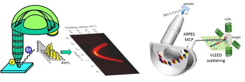
ARPES allows to measure directly the electronic band structure of crystalline solids. Electrons are detected retrieving information about initial state energy, momentum and spin.
IPES probes the empty density of states above the Fermi level of conduction/valence band in condensed matter. Energy of the impinging electron is varied while photons are detected at fixed energy, obtaining the spectrum of the density of unoccupied states. Combined with PES, it gives information on the surface electronic transport gap of sample.